PC16552DVX/NOPB National Semiconductor, PC16552DVX/NOPB Datasheet - Page 12
PC16552DVX/NOPB
Manufacturer Part Number
PC16552DVX/NOPB
Description
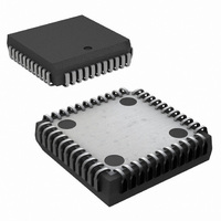
IC UART DUAL WITH FIFO 44-PLCC
Manufacturer
National Semiconductor
Datasheet
1.PC16552DVNOPB.pdf
(22 pages)
Specifications of PC16552DVX/NOPB
Features
False-start Bit Detection
Number Of Channels
2, DUART
Fifo's
16 Byte
Voltage - Supply
5V
With False Start Bit Detection
Yes
With Modem Control
Yes
Mounting Type
Surface Mount
Package / Case
44-LCC (J-Lead)
Leaded Process Compatible
Yes
Rohs Compliant
Yes
Peak Reflow Compatible (260 C)
Yes
Lead Free Status / RoHS Status
Lead free / RoHS Compliant
Other names
*PC16552DVX
*PC16552DVX/NOPB
PC16552DVX
PC16552DVXTR
*PC16552DVX/NOPB
PC16552DVX
PC16552DVXTR
Available stocks
Company
Part Number
Manufacturer
Quantity
Price
Company:

Part Number:
PC16552DVX/NOPB
Manufacturer:
Harwin
Quantity:
34 000
Company:
Part Number:
PC16552DVX/NOPB
Manufacturer:
NSC
Quantity:
3 000
Company:
Part Number:
PC16552DVX/NOPB
Manufacturer:
Texas Instruments
Quantity:
10 000


6 0 Pin Descriptions
RI1 RI2 (Ring Indicator) pins 43 31 When low this indi-
cates that a telephone ringing signal has been received by
the MODEM or data set The RI signal is a MODEM status
input whose condition the CPU can test by reading bit 6 (RI)
of the MODEM Status Register for the appropriate channel
Bit 6 is the complement of the RI signal Bit 2 (TERI) of the
MODEM Status Register indicates whether the RI input sig-
nal has changed from a low to a high state since the previ-
ous reading of the MODEM Status Register
Note Whenever the RI bit of the MODEM Status Register changes from a
SIN1 SIN2 (Serial Input) pins 39 25 Serial data input from
the communications link (peripheral device MODEM or
data set)
SOUT1 SOUT2 (Serial Output) pins 38 26 Composite se-
rial data output to the communications link (peripheral
MODEM or data set) The SOUT signal is set to the Marking
(logic 1) state upon a Master Reset operation
TXRDY1 TXRDY2 (Transmitter Ready) pins 1 32 Trans-
mitter DMA signalling is available through two pins When
operating in the FIFO mode the CPU selects one of
7 0 Connection Diagram
high to a low state an interrupt is generated if the MODEM Status
Interrupt is enabled
(Continued)
See NS Package Number V44A
Order Number PC16552D
Chip Carrier Package
Top View
12
two types of DMA transfer via FCR3 When operating as in
the 16450 Mode only DMA mode 0 is allowed Mode 0
supports single transfer DMA where a transfer is made be-
tween CPU bus cycles Mode 1 supports multi-transfer DMA
where multiple transfers are made continuously until the
XMIT FIFO has been filled Details regarding the active and
inactive states of this signal are given in Section 8 5 Bit 3
V
V
WR (Write) pin 20 When WR is low while the chip is select-
ed the CPU can write control words or data into the select-
ed DUART register
XIN (External Crystal Input) pin 11 This signal input is used
in conjunction with XOUT to form a feedback circuit for the
baud rate generator’s oscillator If a clock signal will be gen-
erated off-chip then it should drive the baud rate generator
through this pin
XOUT (External Crystal Output) pin 13 This signal output is
used in conjunction with XIN to form a feedback circuit for
the baud rate generator’s oscillator If the clock signal will
be generated off-chip then this pin is unused
DD
SS
(Ground) pins 12 22 0V Reference
(Power) pins 33 44
a
5V Supply
TL C 9426– 17
Related parts for PC16552DVX/NOPB
Image
Part Number
Description
Manufacturer
Datasheet
Request
R

Part Number:
Description:
IC UART DUAL WITH FIFO 44-PLCC
Manufacturer:
National Semiconductor
Datasheet:

Part Number:
Description:
UART IC
Manufacturer:
National Semiconductor
Datasheet:

Part Number:
Description:
National Semiconductor [8-Bit D/A Converter]
Manufacturer:
National Semiconductor
Datasheet:
Part Number:
Description:
National Semiconductor [Media Coprocessor]
Manufacturer:
National Semiconductor
Datasheet:
Part Number:
Description:
Digitally Controlled Tone and Volume Circuit with Stereo Audio Power Amplifier, Microphone Preamp Stage and National 3D Sound
Manufacturer:
National Semiconductor
Datasheet:
Part Number:
Description:
Digitally Controlled Tone and Volume Circuit with Stereo Audio Power Amplifier, Microphone Preamp Stage and National 3D Sound
Manufacturer:
National Semiconductor
Datasheet:
Part Number:
Description:
AC97 Rev 2 Codec with Sample Rate Conversion and National 3D Sound
Manufacturer:
National Semiconductor
Part Number:
Description:
Manufacturer:
National Semiconductor
Datasheet:
Part Number:
Description:
Manufacturer:
National Semiconductor
Datasheet:
Part Number:
Description:
General Purpose, Low Voltage, Low Power, Rail-to-Rail Output Operational Amplifiers
Manufacturer:
National Semiconductor
Datasheet:
Part Number:
Description:
8-bit 20 MSPS flash A/D converter.
Manufacturer:
National Semiconductor
Datasheet:
Part Number:
Description:
Low Noise Quad Operational Amplifier
Manufacturer:
National Semiconductor
Datasheet:
Part Number:
Description:
Quad Differential Line Receivers
Manufacturer:
National Semiconductor
Datasheet:
Part Number:
Description:
Quad High Speed Trapezoidal? Bus Transceiver
Manufacturer:
National Semiconductor
Datasheet: