UPA801T-T1-A CALIFORNIA EASTERN LABS, UPA801T-T1-A Datasheet
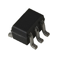
UPA801T-T1-A

Manufacturer Part Number
UPA801T-T1-A
Description
Manufacturer
CALIFORNIA EASTERN LABS
Datasheet

Specifications of UPA801T-T1-A

Transistor Polarity
NPN
Number Of Elements
2
Collector-emitter Voltage
12V
Collector-base Voltage
20V
Emitter-base Voltage
3V
Collector Current (dc) (max)
100mA
Dc Current Gain (min)
70
Power Dissipation
200mW
Frequency (max)
4.5GHz
Operating Temp Range
-65C to 150C
Operating Temperature Classification
Military
Mounting
Surface Mount
Pin Count
6
Package Type
SOT-363
Lead Free Status / Rohs Status
Compliant
• SMALL PACKAGE STYLE:
• LOW NOISE FIGURE:
• HIGH GAIN:
• HIGH COLLECTOR CURRENT: 100mA
NEC's UPA801T is two NPN high frequency silicon epitaxial
transistors encapsulated in an ultra small 6 pin SMT package.
Each transistor is independently mounted and easily config-
ured for either dual transistor or cascode operation. The high
f
suited for pager and other hand-held wireless applications.
ELECTRICAL CHARACTERISTICS
DESCRIPTION
Notes: 1.Pulsed measurement, pulse width ≤ 350 µs, duty cycle ≤ 2 %.
.
FEATURES
T
SYMBOLS
, low voltage bias and small size make this device ideally
h
2 NE856 Die in a 2 mm x 1.25 mm package
NF = 1.2 dB TYP at 1 GHz
|S
|S
FE1
Cre
I
h
I
CBO
EBO
NF
21E
21E
FE 1
f
T
/h
2.The emitter terminal should be connected to the ground terminal of the 3 terminal capacitance bridge.
For Tape and Reel version use part number UPA801T-T1, 3K per reel.
2
FE2
|
2
|
2
= 9.0 dB TYP at 1 GHz
Collector Cutoff Current at V
Emitter Cutoff Current at V
Forward Current Gain at V
Gain Bandwidth at V
Feedback Capacitance at V
Insertion Power Gain at V
Noise Figure at V
h
FE
Ratio: h
PARAMETERS AND CONDITIONS
h
FE1
FE2
PACKAGE OUTLINE
= Smaller Value of Q
= Larger Value pf Q
CE
PART NUMBER
= 3 V, I
CE
= 3 V, I
CE
CE
EB
C
CB
CB
= 3 V, I
FREQUENCY TRANSISTOR
= 7 mA, f = 1 GHz
= 1 V, I
= 3 V, I
C
= 3 V, I
= 10 V, I
= 7 mA
1
C
C
C
1
or Q
= 7 mA, f = 1 GHz
E
or Q
= 0
= 7 mA
= 0, f = 1 MHz
E
(T
= 0
2
A
2
= 25°C)
NPN SILICON HIGH
UNITS
GHz
µA
µA
pF
dB
dB
2.0 ± 0.2
PIN OUT
1. Collector Transistor 1
2. Emitter Transistor 1
3. Collector Transistor 2
4. Emitter Transistor 2
5. Base Transistor 2
6. Base Transistor 1
OUTLINE DIMENSIONS
Note:
Pin 3 is identified with a circle on the bottom of the package.
0.9 ± 0.1
1.3
0.7
0.65
California Eastern Laboratories
0.85
MIN
3.0
70
7
3
2
PACKAGE OUTLINE S06
1
(Top View)
2.1 ± 0.1
1.25 ± 0.1
0 ~ 0.1
UPA801T
TYP
S06
120
4.5
0.7
1.2
9
(Units in mm)
UPA801T
6
5
4
0.2 (All Leads)
0.15
MAX
250
1.0
1.0
1.5
2.5
+0.10
- 0.05

Related parts for UPA801T-T1-A

UPA801T-T1-A Summary of contents

Page 1

... Larger Value pf Q FE2 Notes: 1.Pulsed measurement, pulse width ≤ 350 µs, duty cycle ≤ 2.The emitter terminal should be connected to the ground terminal of the 3 terminal capacitance bridge. For Tape and Reel version use part number UPA801T-T1, 3K per reel. . NPN SILICON HIGH FREQUENCY TRANSISTOR OUTLINE DIMENSIONS 2.0 ± ...

Page 2

... UPA801T ABSOLUTE MAXIMUM RATINGS SYMBOLS PARAMETERS V Collector to Base Voltage CBO V Collector to Emitter Voltage CEO V Emitter to Base Voltage EBO I Collector Current C P Total Power Dissipation T 1 Die 2 Die T Junction Temperature J T Storage Temperature STG Note: 1. Operation in excess of any one of these parameters may result in permanent damage ...

Page 3

... Collector Current FEED BACK CAPACITANCE vs. COLLECTOR TO BASE VOLTAGE 5 MHz 2.0 1.0 0.5 0.2 0 Collector to Base Voltage 25° GHz 50 (mA GHz 50 100 (mA (V) CB UPA801T INSERTION POWER GAIN vs. COLLECTOR CURRENT GHz 0 100 Collector Current, I (mA) C INSERTION POWER GAIN vs. FREQUENCY 0.1 0.2 0.5 1.0 2 ...

Page 4

... UPA801T TYPICAL SCATTERING PARAMETERS UPA801T mA Ω Ω Ω Ω Ω FREQUENCY S 11 (GHz) MAG ANG 0.10 .967 -22.9 0.20 .930 -45.8 0.30 .884 -67.1 0.40 .842 -86.9 0.50 .801 -103.1 0.60 .771 -117.0 0.70 .742 -130.0 0.80 .722 -141.2 0.90 .706 -151 ...

Page 5

... ORDERING INFORMATION PART NUMBER QUANTITY UPA801T-T1-A 3000 (T = 25° MAG ANG MAG ANG 8.934 148.0 .038 65.8 8.007 127.6 .060 53.1 6.898 112 ...

Page 6

NONLINEAR MODEL BJT NONLINEAR MODEL PARAMETERS Parameters Q1, Q2 Parameters IS 6e-16 MJC BF 120 XCJC NF 0.98 CJS VAF 10 VJS IKF 0.08 MJS ISE 32e- 1. XTF NR 0.991 VTF VAR 3.9 ITF ...

Page 7

NONLINEAR MODEL SCHEMATIC LC Pin_1 0.05 nH C_C1E1 0. Pin_2 0. Pin_3 0.05 nH Life Support Applications These NEC products are not intended for use in life support devices, appliances, or systems where the malfunction of ...

Page 8

Subject: Compliance with EU Directives CEL certifies, to its knowledge, that semiconductor and laser products detailed below are compliant with the requirements of European Union (EU) Directive 2002/95/EC Restriction on Use of Hazardous Substances in electrical and electronic equipment (RoHS) ...

Related keywords