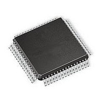
SI3220-FQ Silicon Laboratories Inc, SI3220-FQ Datasheet - Page 4

SI3220-FQ
Manufacturer Part Number
SI3220-FQ
Description
IC SLIC/CODEC DUAL-CH 64TQFP
Manufacturer
Silicon Laboratories Inc
Series
ProSLIC®r
Specifications of SI3220-FQ
Function
Subscriber Line Interface Concept (SLIC), CODEC
Interface
GCI, PCM, SPI
Number Of Circuits
2
Voltage - Supply
3.3V, 5V
Current - Supply
65mA
Power (watts)
941mW
Operating Temperature
0°C ~ 70°C
Mounting Type
Surface Mount
Package / Case
*
Includes
Battery Switching, BORSCHT Functions, DTMF Generation and Decoding, FSK Tone Generation, Modem and Fax Tone Detection
Product
Telecom
Lead Free Status / RoHS Status
Lead free / RoHS Compliant
Available stocks
Company
Part Number
Manufacturer
Quantity
Price
Company:
Part Number:
SI3220-FQ
Manufacturer:
Silicon Laboratories Inc
Quantity:
10 000
Part Number:
SI3220-FQ
Manufacturer:
N/A
Quantity:
20 000
Company:
Part Number:
SI3220-FQR
Manufacturer:
SILICON
Quantity:
12 000
Table 1. Absolute Maximum Ratings and Thermal Information
Si3220/Si3225
Electrical Specifications
Parameter
Supply Voltage, Si3200 and Si3220/Si3225
High Battery Supply Voltage, Si3200
Low Battery Supply Voltage, Si3200
TIP or RING Voltage, Si3205
TIP, RING Current, Si3200
STIPAC, STIPDC, SRINGAC, SRINGDC Current,
Si3220/Si3225
Input Current, Digital Input Pins
Si3220/25 Analog Ground Differential Voltage
(GND1 to ePad, GND2 to ePad, or GND1 to GND2)
Si3220/25 Digital Ground Differential Voltage (GND3
to GND4)
Si3220/25 Analog to Digital Ground Differential Volt-
age (GND1/GND2/ePad to GND3/GND4)
Digital Input Voltage
Operating Temperature Range
Storage Temperature Range
Si3220/Si3225 Thermal Resistance, Typical
(TQFP-64 ePad)
Si3200 Thermal Resistance, Typical
ePad)
Continuous Power Dissipation, Si3200
Continuous Power Dissipation, Si3220/25
Notes:
4
1. Permanent device damage may occur if the above Absolute Maximum Ratings are exceeded. Functional operation
2. The dv/dt of the voltage applied to the VBAT, VBATH, and VBATL pins must be limited to 10 V/µs.
3. The thermal resistance of an exposed pad package is assured when the recommended printed circuit board layout
4. On-chip thermal limiting circuitry will shut down the circuit at a junction temperature of approximately 150 °C. For optimal
5. The PCB pad placed under the device package must be connected with multiple vias to the PCB ground layer and to the
should be restricted to the conditions as specified in the operational sections of this data sheet. Exposure to absolute
maximum rating conditions for extended periods may affect device reliability.
guidelines are followed correctly. The specified performance requires that the exposed pad be soldered to an exposed
copper surface of equal size and that multiple vias are added to enable heat transfer between the top-side copper
surface and a large internal copper ground plane. Refer to “AN55: Dual ProSLIC
evaluation board data sheet for specific layout examples.
reliability, junction temperatures above 140 °C should be avoided.
GND1-GND4 pins via short traces. The TQFP-64 e-Pad must be properly soldered to the PCB pad during PCB
assembly. This type of low-impedance grounding arrangement is necessary to ensure that maximum differentials are not
exceeded under any operating condition in addition to providing thermal dissipation.
5
3
2
(SOIC-16
4
5
3
5
Rev. 1.0
V
DD
∆V
V
V
I
Symbol
∆V
∆V
, V
TIP
BAT
TIP
V
GND,A–D
T
V
θ
θ
DD1
BATH
, I
P
P
I
GNDD
T
,V
GNDA
STG
,V
IND
IN
JA
JA
A
D
D
RING
RING
BATL
–V
DD4
Pulse < 10 µs
1
Pulse < 4 µs
Continuous
Continuous
Continuous
Continuous
T
T
Condition
TQFP-64
A
SOIC-16
A
10 ms
= 85 °C,
= 85 °C,
Test
®
User Guide” or to the Si3220/3225
–0.3 to (
0.4 to –104
0.4 to –109
–0.5 to 6.0
–40 to 100
–40 to 150
V
V
BATH
BATH
Value
V
–104
±100
±200
±20
±10
±50
±50
V
1.6
BATH
25
55
1
DDD
–15
–35
+ 0.3)
°C/W
°C/W
Unit
mA
mA
mA
mV
mV
mV
°C
°C
W
W
V
V
V
V


