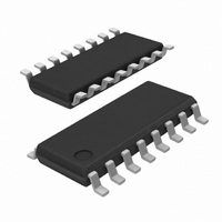
SI3018-FS Silicon Laboratories Inc, SI3018-FS Datasheet - Page 36

SI3018-FS
Manufacturer Part Number
SI3018-FS
Description
IC VOICE DAA GCI/PCM/SPI 16SOIC
Manufacturer
Silicon Laboratories Inc
Datasheet
1.SI3018-FS.pdf
(94 pages)
Specifications of SI3018-FS
Function
Data Access Arrangement (DAA)
Interface
Serial
Number Of Circuits
1
Voltage - Supply
3 V ~ 3.6 V
Current - Supply
8.5mA
Operating Temperature
0°C ~ 70°C
Mounting Type
Surface Mount
Package / Case
16-SOIC (3.9mm Width)
Includes
Line Voltage Monitor, Loop Current Monitor, Overload Detection, Parallel Handset Detection, Polarity Reversal Detection, TIP and
Lead Free Status / RoHS Status
Lead free / RoHS Compliant
Power (watts)
-
Available stocks
Company
Part Number
Manufacturer
Quantity
Price
Company:
Part Number:
SI3018-FS
Manufacturer:
SILICO
Quantity:
8 436
Company:
Part Number:
SI3018-FS
Manufacturer:
SILICON41
Quantity:
1 010
Part Number:
SI3018-FS
Manufacturer:
SILICON LABS/芯科
Quantity:
20 000
Company:
Part Number:
SI3018-FSR
Manufacturer:
FSC
Quantity:
20 000
Part Number:
SI3018-FSR
Manufacturer:
SILICON LABS/芯科
Quantity:
20 000
Si3018/19/10
5.24. Filter Selection
The Si3056 supports additional filter selections for the
receive and transmit signals as defined in Table 11 and
Table 12 on page 15. The IIRE bit (Register 16, bit 4)
selects between the IIR and FIR filters. The IIR filter
provides a shorter, but non-linear, group delay
alternative to the default FIR filter and only operates
with an 8 kHz sample rate. Also, on the Si3019 line-side
device, the FILT bit (Register 31, bit 1) selects a –3 dB
low frequency pole of 5 Hz when cleared and 200 Hz
when set. The FILT bit affects the receive path only.
5.25. Clock Generation
The Si3056 has an on-chip clock generator. Using a
single MCLK input frequency, the Si3056 generates all
the desired standard modem sample rates.
The clock generator consists of two phase-locked loops
(PLL1 and PLL2) that achieve the desired sample
frequencies. Figure 26 illustrates the clock generator.
The architecture of the dual PLL scheme provides fast
lock time on initial start-up, fast lock time when
changing modem sample rates, high noise immunity,
and can change modem sample rates with a single
register write. Many MCLK frequencies between
1 and 60 MHz are supported. MCLK should be from a
clean source, preferably directly from a crystal with a
constant frequency and no dropped pulses.
In serial mode 2 (refer to the “5.26.Digital Interface”
section), the Si3056 operates as a slave device. The
clock generator is configured based on the SRC register
to generate the required internal clock frequencies. In
this mode, PLL2 is powered-down. For further details of
slave mode operation, see "5.27.Multiple Device
Support" on page 38.
5.25.1. Programming the Clock Generator
As shown in Figure 26, PLL1 must output a clock equal
to 98.304 MHz (F
programming the following registers:
The main design consideration is the generation of a
base frequency, defined as follows:
36
Register 8: PLL1 N[7:0] divider.
Register 9: PLL1 M[7:0] divider.
F BASE
BASE
=
F
---------------------------- -
MCLK
). The F
N
×
M
=
BASE
98.304 MHz
is determined by
Rev. 1.05
N (Register 8) and M (Register 9) are 8-bit unsigned
values. F
the MCLK pin.
Table 20 lists several standard crystal oscillator rates
that can be supplied to MCLK. This list represents a
sample of MCLK frequency choices. Many others are
possible.
After PLL1 is programmed, the SRC[3:0] bits can
achieve the standard modem sampling rates with a
single write to Register 7. See "Register 7.Sample Rate
Control" on page 54.
When programming the registers of the clock generator,
the order of register writes is important. For PLL1
updates, N (Register 8, bits 7:0) must be written first,
then immediately followed by a write to M (Register 9,
bits 7:0).
The values shown in Table 20 satisfy the preceding
equation. However, when programming the registers for
N and M, the value placed in these registers must be
one less than the value calculated from the equations.
For example, with an MCLK of 46.08 MHz, the values
placed in the N and M registers are 0x0Dh and 0x1Fh,
respectively.
MCLK
MCLK (MHz)
10.3680
11.0592
14.7456
18.4320
24.5760
25.8048
44.2368
46.0800
47.9232
56.0000
Table 20. MCLK Examples
1.8432
4.0960
6.1440
8.1920
9.2160
12.288
is the frequency of the clock provided to
27
21
15
39
35
N
3
1
1
1
3
9
1
3
3
1
9
160
256
24
16
12
32
80
20
16
80
20
32
80
36
M
8
4


