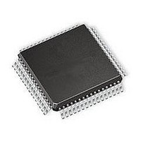
SI3225-KQ Silicon Laboratories Inc, SI3225-KQ Datasheet - Page 46

SI3225-KQ
Manufacturer Part Number
SI3225-KQ
Description
IC SLIC/CODEC DUAL-CH 64TQFP
Manufacturer
Silicon Laboratories Inc
Series
ProSLIC®r
Specifications of SI3225-KQ
Package / Case
*
Function
Subscriber Line Interface Concept (SLIC), CODEC
Interface
GCI, PCM, SPI
Number Of Circuits
2
Voltage - Supply
3.3V, 5V
Current - Supply
65mA
Power (watts)
941mW
Operating Temperature
0°C ~ 70°C
Mounting Type
Surface Mount
Includes
Battery Switching, BORSCHT Functions, DTMF Generation and Decoding, FSK Tone Generation, Modem and Fax Tone Detection
Product
SLIC
Supply Voltage (min)
3.13 V
Supply Current
22 mA
Maximum Operating Temperature
+ 70 C
Minimum Operating Temperature
0 C
Mounting Style
SMD/SMT
Number Of Channels
2
Lead Free Status / RoHS Status
Contains lead / RoHS non-compliant
Available stocks
Company
Part Number
Manufacturer
Quantity
Price
Company:
Part Number:
SI3225-KQ
Manufacturer:
Silicon Laboratories Inc
Quantity:
10 000
Notes:
(Si3220)
(Si3225)
Ringing
External
Method
Internal
Si3220/Si3225
Loop Closure Mask
The Dual ProSLIC implements a loop closure mask to
ensure mode change between Ringing and Active or
On-hook Transmission without causing an erroneous
loop closure detection. The loop closure mask register,
LCRMASK, should be set such that loop closure
detection is ignored for LCRMASK 1.25 ms/LSB
amount of time. The programmed time is set to mask
detection of transitional currents that occur when exiting
the ringing mode while driving a reactive load (i.e., 5
REN). A typical setting is 80 ms (LCRMASK = 0x40).
Si3220 Ring Trip Detection
The Si3220 provides the ability to process a ring trip
event using an ac-based detection scheme. Using this
scheme eliminates the need to add dc offset to the
46
1. All calculated values should be rounded to the nearest integer.
2. Refer to Ring Trip Debounce Interval for RTACDB and RTDCDB equations.
Ring Trip Interrupt Pending
Ring Trip Interrupt Enable
AC Ring Trip Threshold
DC Ring Trip Threshold
Ring Trip Sample Period
Linefeed Shadow (monitor only)
Ring Trip Detect Status
(monitor only)
AC Ring Trip Detect Debounce
Interval
DC Ring Trip Detect Debounce
Interval
Loop Current Sense
(monitor only)
Frequency
16–32 Hz
33–60 Hz
16–32 Hz
33–60 Hz
Ringing
Table 26. Recommended Values for Ring Trip Registers and RAM Addresses
Parameter
Table 27. Register and RAM Locations Used for Ring Trip Detection
Added?
Offset
Yes
Yes
Yes
Yes
DC
No
No
2(800/f
2(800/f
2(800/f
800/f
800/f
800/f
RTPER
Register/RAM
RING
RING
RING
Mnemonic
LINEFEED
RING
RING
RING
IRQVEC2
RTDCDB
RTDCTA
LCRRTP
RTACDB
RTACTH
IRQEN2
RTPER
ILOOP
)
)
)
Preliminary Rev. 0.91
1.59 x V
1.59 x V
221 x RTPER
221 x RTPER
RTDCTH[15:0]
RTDCDB[15:0]
Register/RAM
RTACDB[15:0]
RTACTH[15:0]
RTACTH
RING,PK
RING,PK
RTPER[15:0]
ILOOP[15:0]
32767
32767
ringing signal, which reduces the total power dissipation
during the ringing state and maximizes the available
ringing amplitude. This scheme is valid for shorter loop
lengths only since it cannot reliably detect a ring trip
event if the off-hook line impedance overlaps the on-
hook impedance at 20 Hz.
The Si3220 also can add a dc offset component to the
ringing signal and detect a ring trip event by monitoring
the dc loop current flowing once the terminal equipment
transitions to the off-hook state. Although adding dc
offset reduces the maximum available ringing amplitude
(using the same ringing supply), this method is required
to reliably detect a valid ring trip event when sourcing
longer loop lengths. The dc offset can be programmed
from 0 to 64.32 V in the RINGOF RAM address as
LFS[2:0]
RTRIPS
RTRIPE
RTP
Bits
x RTPER
x RTPER
Enabled/Disabled
Programmable
0 to 101.09 mA
0.067 x RTPER x V
0.067 x RTPER x V
See Table 26
See Table 26
See Table 26
0.577(RTPER x V
0.577(RTPER x V
0 to 40.96 s
0 to 40.96 s
Yes/No
Range
N/A
N/A
RTDCTH
32767
32767
OFF
OFF
OFF
OFF
)
)
Resolution
1
Table 19
1.25 ms
1.25 ms
See
N/A
N/A
N/A
N/A
See Note
RTACDB/
RTDCDB
2


