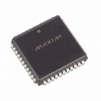
MAX456EQH+TD Maxim Integrated Products, MAX456EQH+TD Datasheet - Page 5

MAX456EQH+TD
Manufacturer Part Number
MAX456EQH+TD
Description
IC VIDEO CROSSPOINT SWIT 44PLCC
Manufacturer
Maxim Integrated Products
Datasheet
1.MAX456CPL.pdf
(12 pages)
Specifications of MAX456EQH+TD
Function
Video Crosspoint Switch
Circuit
1 x 8:8
Operating Temperature
-40°C ~ 85°C
Mounting Type
Surface Mount
Package / Case
44-LCC (J-Lead)
Lead Free Status / RoHS Status
Lead free / RoHS Compliant
The MAX456 video crosspoint switch consists of 64
T-switches in an 8 x 8 grid (Figure 1). The 8 matrix out-
puts are followed by 8 wideband buffers optimized for
driving 400Ω and 20pF loads. Each buffer has an
internal active load on the output that can be readily
shut off via the LOAD input (off when LOAD = 0V). The
shut-off is useful when two or more MAX456 circuits are
connected in parallel to create more input channels.
With more input channels, only one set of buffers can
be active and only one set of loads can be driven.
And, when active, the buffer must have either
1) an internal load, 2) the internal load of another buffer
in another MAX456, or 3) an external load.
Each MAX456 output can be disabled under logic con-
trol. When a buffer is disabled, its output enters a high-
impedance state. In multichip parallel applications, the
disable function prevents inactive outputs from loading
lines driven by other devices. Disabling the inactive
buffers reduces power consumption.
The MAX456 outputs connect easily to MAX470 quad,
gain-of-two buffers when 75Ω loads must be driven.
The MAX456 has an internal power-on reset (POR) cir-
cuit that remains low for 5µs when power is applied.
POR also remains low if the total supply voltage is less
than 4V. The POR disables all buffer outputs at
power-up, but the switch matrix is not preset to any ini-
tial condition. The desired switch state should be pro-
grammed before the buffer outputs are enabled.
_______________Detailed Description
_______________________________________________________________________________________
Power-On RESET
Output Buffers
8 x 8 Video Crosspoint Switch
The desired switch state can be loaded in a 7-bit paral-
lel-interface mode or 32-bit serial-interface mode (see
Table 3 and Figures 4-6). All action associated with the
WR line occurs on its rising edge. The same is true for
the LATCH line if EDGE/
second-rank registers update while LATCH is low
(when EDGE/
CE and
enable.
In the parallel-interface mode, the 7 data bits A2-A0
and D3-D0 specify an output channel (A2-A0) and the
input channel to which it connects (D3-D0). The data is
loaded on the rising edge of WR. The 8 input channels
are selected by 0000 through 0111 (D3-D0). The
remaining 8 codes (1000-1111) control other MAX456
functions, as listed in Table 1.
In serial mode (SER/
are loaded with data, making it unnecessary to specify
an output address (A2, A1, A0). The input data format
is D3-D0, starting with OUT0 and ending with OUT7 for
32 total bits. Only codes 0000 through 1010 are valid.
Code 1010 disables a buffer, while code 1001 enables
it. After data is shifted into the 32-bit first-rank register,
it is transferred to the second rank by the LATCH line
(see Table 2).
___________________Digital Interface
–
C
—
E
–
to allow active-high or active-low chip
–
L
—
E
—
V
—
E
—
L
–
32-Bit Serial-Interface Mode
is low). WR is logically ANDed with
–
P
—
A
—
R
–
–
L
—
= high), all first-rank registers
E
—
V
—
E
—
L
–
7-Bit Parallel Mode
is high. Otherwise, the
5


