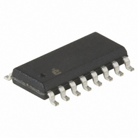
ISL84522IB Intersil, ISL84522IB Datasheet - Page 8

ISL84522IB
Manufacturer Part Number
ISL84522IB
Description
IC SWITCH QUAD SPST 16SOIC
Manufacturer
Intersil
Datasheet
1.ISL84522IVZ.pdf
(12 pages)
Specifications of ISL84522IB
Function
Switch
Circuit
4 x SPST - NO
On-state Resistance
100 Ohm
Voltage Supply Source
Single, Dual Supply
Voltage - Supply, Single/dual (±)
±2 V ~ 6 V, 2 V ~ 12 V
Current - Supply
.05µA
Operating Temperature
-40°C ~ 85°C
Mounting Type
Surface Mount
Package / Case
16-SOIC (0.154", 3.90mm Width)
Lead Free Status / RoHS Status
Contains lead / RoHS non-compliant
Available stocks
Company
Part Number
Manufacturer
Quantity
Price
Part Number:
ISL84522IBZ
Manufacturer:
INTERSIL
Quantity:
20 000
Company:
Part Number:
ISL84522IBZ-T
Manufacturer:
INTERSIL
Quantity:
14 881
V+ and GND power the internal logic (thus setting the digital
switching point) and level shifters. The level shifters convert
the logic levels to switched V+ and V- signals to drive the
analog switch gate terminals, so switch parameters -
especially R
Logic-Level Thresholds
V+ and GND power the internal logic stages, so V- has no
affect on logic thresholds. This switch family is TTL
compatible (0.8V and 2.4V) over a V+ supply range of 2.5V
to 10V. At 12V the V
use a logic family the provides a V
The digital input stages draw supply current whenever the
digital input voltage is not at one of the supply rails. Driving
the digital input signals from GND to V+ with a fast transition
time minimizes power dissipation.
High-Frequency Performance
In 50Ω systems, signal response is reasonably flat even past
300MHz (Figure 15), with a small signal -3dB bandwidth in
excess of 400MHz, and a large signal bandwidth exceeding
300MHz.
An off switch acts like a capacitor and passes higher
frequencies with less attenuation, resulting in signal
feedthrough from a switch’s input to its output. OFF Isolation
is the resistance to this feedthrough, while Crosstalk
indicates the amount of feedthrough from one switch to
Typical Performance Curves
250
200
150
100
90
80
70
60
50
50
40
0
FIGURE 9. ON RESISTANCE vs SUPPLY VOLTAGE
3
-40
ON
85
4
o
o
C
C
- are strong functions of both supplies.
5
IH
25
level is about 2.7V, so for best results
o
6
C
V- = 0V
V- = -5V
8
7
V+ (V)
OH
8
-40
85
25
greater than 3V.
o
o
o
C
C
C
9
T
A
ISL84521, ISL84522, ISL84523
V
I
= 25
COM
COM
10
o
= 1mA
C, Unless Otherwise Specified
= (V+) - 1V
11
12
another. Figure 16 details the high OFF Isolation and
Crosstalk rejection provided by this family. At 10MHz, OFF
isolation is about 50dB in 50Ω systems, decreasing
approximately 20dB per decade as frequency increases.
Higher load impedances decrease OFF Isolation and
Crosstalk rejection due to the voltage divider action of the
switch OFF impedance and the load impedance.
Leakage Considerations
Reverse ESD protection diodes are internally connected
between each analog-signal pin and both V+ and V-. One
of these diodes conducts if any analog signal exceeds V+
or V-.
Virtually all the analog leakage current comes from the ESD
diodes to V+ or V-. Although the ESD diodes on a given
signal pin are identical and therefore fairly well balanced,
they are reverse biased differently. Each is biased by either
V+ or V- and the analog signal. This means their leakages
will vary as the signal varies. The difference in the two diode
leakages to the V+ and V- pins constitutes the analog-signal-
path leakage current. All analog leakage current flows
between each pin and one of the supply terminals, not to the
other switch terminal. This is why both sides of a given
switch can show leakage currents of the same or opposite
polarity. There is no connection between the analog signal
paths and GND.
300
250
200
150
100
225
175
125
140
110
FIGURE 10. ON RESISTANCE vs SWITCH VOLTAGE
50
75
80
50
0
85
25
o
C
o
C
1
2
V
V+ = 5V
COM
(V)
85
25
-40
3
o
o
o
C
V- = 0V
C
C
85
25
-40
o
o
o
C
C
C
I
COM
4
V+ = 2.7V
V- = 0V
-40
V+ = 3.3V
V- = 0V
= 1mA
o
C
5


