SY55858UHI Micrel Inc, SY55858UHI Datasheet - Page 6
SY55858UHI
Manufacturer Part Number
SY55858UHI
Description
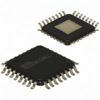
IC CROSSPOINT SWITCH DUAL 32TQFP
Manufacturer
Micrel Inc
Series
SY55r
Datasheet
1.SY55858UHG.pdf
(8 pages)
Specifications of SY55858UHI
Function
Crosspoint Switch
Circuit
2 x 2:2
Voltage Supply Source
Single Supply
Voltage - Supply, Single/dual (±)
2.3 V ~ 3.6 V
Current - Supply
150mA
Operating Temperature
-40°C ~ 85°C
Mounting Type
Surface Mount
Package / Case
32-TQFP Exposed Pad
Array Configuration
2x2
Differential Data Transmission
Yes
Power Supply Requirement
Single
Pin Count
32
Mounting
Surface Mount
Operating Temperature (max)
85C
Operating Temperature (min)
-40C
Operating Temperature Classification
Industrial
Cascading Capability
No
Line Code
NRZ
On-chip Buffers
Yes
On-chip Decoder
No
On-chip Latch Circuit
No
On-chip Mux/demux
No
Programmable
No
Operating Supply Voltage (max)
3.6V
Dual Supply Voltage (typ)
Not RequiredV
Dual Supply Voltage (max)
Not RequiredV
Dual Supply Voltage (min)
Not RequiredV
Output Level
CML
Lead Free Status / RoHS Status
Contains lead / RoHS non-compliant
Available stocks
Company
Part Number
Manufacturer
Quantity
Price
Company:

Part Number:
SY55858UHI
Manufacturer:
MICREL
Quantity:
820


V
Note 3.
Note 4.
Micrel, Inc.
V
Note 5.
Note 6.
Note 7.
Note 8.
Note 9.
M9999-110705
hbwhelp@micrel.com or (408) 955-1690
Symbol
V
R
V
V
V
V
V
R
Symbol
f
t
t
t
t
R
D
t
CC
CC
MAX
PLH
PHL
SWITCH
SKEW
r
CML DC ELECTRICAL CHARACTERISTICS
OUT(SWING)
AC ELECTRICAL CHARACTERISTICS
, t
ID
IN
IH
IL
OH
OL
OUT
J
J
f
= 2.3V to 3.6V; GND = 0V; T
= 2.3V to 3.6V; GND = 0V; T
Device is guaranteed to meet the DC specifications, shown in the table above, after thermal equilibrium has been established. The device is
tested in a socket such that traverse airflow 500lfpm is maintained.
V
purposes is 2
swing is available in the 50 environment. Refer to the “CML Output Termination Application” section, Figures 3 and 4, for more details.
Tested using environment of Figure 3, 50 equivalent load. AC parameters are guaranteed by design and characterization.
f
equivalent load.
Input TTL/CMOS edge rate of <1.5ns.
Worst-case difference between QA0 and QA1 from either DA0 or DA1 (or between QB0 and QB1 from either DB0 or DB1 respectively), when
both outputs come from the same input.
Worst-case difference between QA and QB outputs, when DA or DB inputs are shorted.
MAX
OUT(SWING)
Maximum Frequency
Differential Propagation Delay
Select-to-Valid Output
Within-Device Skew
Within-Device Skew
Part-to-Part Skew (Diff.)
Random Jitter
Deterministic Jitter
CML Output Rise/Fall Times
(20% to 80%)
clock is defined as the maximum toggle rate the device can operate while still achieving a 250mV minimum CML output swing, 50
Differential Input Voltage
Differential Input Resistance
Input HIGH Voltage
Input LOW Voltage
Output HIGH Voltage
Output LOW Voltage
Output Voltage Swing
Output Source Impedance
is defined as the swing on one output of a differential pair, that is |V
Parameter
Clock Frequency
Parameter
V
OUT(SWING)
NRZ Data Rate
(8)
(9)
D-to-/D
D-to-Q
. Actual voltage levels and differential swing will depend on customer termination scheme. Typically, a 400mV
(7)
(4)
A
A
(6)
= –40 C to +85 C
= –40 C to +85 C
V
V
CC
CC
Min.
0.650
220
3.0
3.0
Min.
—
—
—
—
—
—
—
100
1.6
1.5
– 0.040
90
40
—
– 1.00
(3)
(5)
V
V
CC
CC
6
Typ.
0.50
350
100
0.800
0.400
12
25
80
—
—
Typ.
2
5
100
– 0.010
– 0.800
—
—
—
50
OH
– V
V
V
CC
Max.
450
120
1.0
OL
—
—
25
50
—
20
CC
5
Max.
V
V
1.00
110
– 0.650
| on one pin. The swing for common mode immunity
60
—
—
CC
CC
– 0.1
ps
Gbps
ps
Unit
GHz
Unit
ps
ns
ps
ps
ps
mV
RMS
V
V
V
V
V
PP
50
Condition
No Load
No Load
No Load
Environment
Condition
SuperLite™
SY55858U
Related parts for SY55858UHI
Image
Part Number
Description
Manufacturer
Datasheet
Request
R

Part Number:
Description:
IC TRANSLATOR DUAL LVDS 10MSOP
Manufacturer:
Micrel Inc
Datasheet:
Part Number:
Description:
IC TRANSLATOR DUAL LVPECL 10MSOP
Manufacturer:
Micrel Inc
Datasheet:

Part Number:
Description:
IC XPOINT SWITCH 2X2 PROT 16QSOP
Manufacturer:
Micrel Inc
Datasheet:
Part Number:
Description:
IC XPOINT SWITCH 2X2 PROT 16QSOP
Manufacturer:
Micrel Inc
Datasheet:

Part Number:
Description:
IC CROSSPOINT SWITCH DUAL 32TQFP
Manufacturer:
Micrel Inc
Datasheet:
Part Number:
Description:
IC CROSSPOINT SWITCH DUAL 32TQFP
Manufacturer:
Micrel Inc
Datasheet:

Part Number:
Description:
IC CROSSPOINT SWITCH DUAL 32MLF
Manufacturer:
Micrel Inc
Datasheet:
Part Number:
Description:
IC CROSSPOINT SWITCH 2X2 16-QSOP
Manufacturer:
Micrel Inc
Datasheet:
Part Number:
Description:
IC CROSSPOINT SWITCH DUAL 32TQFP
Manufacturer:
Micrel Inc
Datasheet:
Part Number:
Description:
IC CROSSPOINT SWITCH DUAL 32MLF
Manufacturer:
Micrel Inc
Datasheet:
Part Number:
Description:
IC FLIP FLOP D 2.5GHZ 10-MSOP
Manufacturer:
Micrel Inc
Datasheet:
Part Number:
Description:
IC FLIP FLOP D 2.5GHZ 10-MSOP
Manufacturer:
Micrel Inc
Datasheet:
Part Number:
Description:
IC GATE UNIV 3GHZ 50 OHM 10-MSOP
Manufacturer:
Micrel Inc
Datasheet:

Part Number:
Description:
IC GATE CML UNIV I/O TERM 16MLF
Manufacturer:
Micrel Inc
Datasheet:
Part Number:
Description:
IC GATE UNIV 3GHZ 50 OHM 10MSOP
Manufacturer:
Micrel Inc
Datasheet: