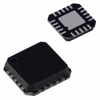
ADG784BCP-REEL Analog Devices Inc, ADG784BCP-REEL Datasheet - Page 3

ADG784BCP-REEL
Manufacturer Part Number
ADG784BCP-REEL
Description
IC MUX/DEMUX QUAD 2X1 20LFCSP
Manufacturer
Analog Devices Inc
Datasheet
1.ADG784BCPZ-REEL.pdf
(8 pages)
Specifications of ADG784BCP-REEL
Rohs Status
RoHS non-compliant
Function
Multiplexer/Demultiplexer
Circuit
4 x 2:1
On-state Resistance
5 Ohm
Voltage Supply Source
Single Supply
Voltage - Supply, Single/dual (±)
1.8 V ~ 5.5 V
Current - Supply
1µA
Operating Temperature
-40°C ~ 85°C
Mounting Type
Surface Mount
Package / Case
20-VFQFN, CSP Exposed Pad
SINGLE SUPPLY
Parameter
ANALOG SWITCH
LEAKAGE CURRENTS
DIGITAL INPUTS
DYNAMIC CHARACTERISTICS
POWER REQUIREMENTS
NOTES
1
2
Specifications subject to change without notice.
Temperature ranges are as follows: B Version, –40°C to +85°C.
Guaranteed by design, not subject to production test.
Analog Signal Range
On Resistance (R
On Resistance Match Between
On Resistance Flatness (R
Source OFF Leakage I
Drain OFF Leakage I
Channel ON Leakage I
Input High Voltage, V
Input Low Voltage, V
Input Current
t
t
Break-Before-Make Time Delay, t
Off Isolation
Channel-to-Channel Crosstalk
Bandwidth –3 dB
Distortion
Charge Injection
C
C
C
I
I
I
ON
OFF
DD
IN
O
S
D
D
Channels (∆R
I
INL
(OFF)
, C
(OFF)
S
or I
(ON)
INH
ON
ON
)
)
D
INL
INH
S
(V
D
(OFF)
(OFF)
, I
DD
FLAT(ON)
S
= 3 V
(ON)
EN
1
0
0
2
D
)
10%, GND = 0 V. All specifications T
IN
X
0
1
25 C
4
0.15
2
± 0.01
± 0.5
± 0.01
± 0.5
± 0.01
± 0.5
0.001
0.001
D1
Hi-Z
S1A
S1B
B Version
240
T
T
0 V to V
10
0.5
4
± 1
± 1
± 1
2.0
0.4
± 0.5
12
25
5
10
5
1
–65
–75
2
3
10
20
30
1
1
100
MIN
MAX
Table I. Truth Table
D2
Hi-Z
S2A
S2B
to
DD
D3
Hi-Z
S3A
S3B
Unit
V
Ω typ
Ω max
Ω typ
Ω max
Ω typ
Ω max
nA typ
nA max
nA typ
nA max
nA typ
nA max
V min
V max
µA typ
µA max
ns typ
ns max
ns typ
ns max
ns typ
ns min
dB typ
dB typ
MHz typ
% typ
pC typ
pF typ
pF typ
pF typ
µA max
µA typ
µA typ
mA max
MIN
to T
D4
Hi-Z
S4A
S4B
MAX
unless otherwise noted.)
Test Conditions/Comments
V
V
V
V
Test Circuit 2
V
Test Circuit 2
V
V
R
V
R
V
R
V
R
R
R
R
C
f = 1 kHz
f = 1 kHz
f = 1 MHz
V
Digital Inputs = 0 V or V
V
V
Function
DISABLE
IN = 0
IN = 1
D
D
D
D
D
D
IN
L
S
L
S
L
S1
L
L
L
L
DD
IN
S
L
/V
= 1.5 V; Test Circuit 4
= 1.5 V; Test Circuit 4
= 100 Ω, C
= 100 Ω, C
= 100 Ω, C
= 50 Ω, f = 10 MHz; Test Circuit 7
= 50 Ω, f = 10 MHz; Test Circuit 8
= 50 Ω; Test Circuit 6
= 50 Ω
= 1 nF; Test Circuit 9
= 0 V to V
= 0 V to V
= 0 V to V
= 3 V, V
= 3 V, V
= V
= V
= V
= 3 V
= 3.3 V
D
= 0 V
S
INL
S2
= 3 V; V
= 3 V; Test Circuit 5
or V
S
S
= 1 V; V
= 1 V; V
DD
DD
DD
L
L
L
INH
= 35 pF,
= 35 pF,
= 35 pF,
, I
, I
, I
D
S
S
S
= V
= –10 mA
= –10 mA
= –10 mA
D
D
S
= 1 V, V
= 1 V, V
= 1 V; Test Circuit 3
DD
S
S
= 3 V;
= 3 V;
ADG784


