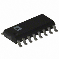
ADG512BR Analog Devices Inc, ADG512BR Datasheet - Page 6

ADG512BR
Manufacturer Part Number
ADG512BR
Description
IC SWITCH QUAD SPST 16SOIC
Manufacturer
Analog Devices Inc
Series
LC²MOSr
Type
Analog Switchr
Datasheet
1.ADG512BRZ.pdf
(12 pages)
Specifications of ADG512BR
Rohs Status
RoHS non-compliant
Function
Switch
Circuit
4 x SPST - NC
On-state Resistance
30 Ohm
Voltage Supply Source
Single, Dual Supply
Voltage - Supply, Single/dual (±)
3V, ±5V
Current - Supply
0.0001µA
Operating Temperature
-40°C ~ 85°C
Mounting Type
Surface Mount
Package / Case
16-SOIC (0.154", 3.90mm Width)
Multiplexer Configuration
Quad SPST
Number Of Inputs
4
Number Of Outputs
4
Number Of Channels
4
Analog Switch On Resistance
200@3VOhm
Analog Switch Turn On Time
600ns
Analog Switch Turn Off Time
120ns
Package Type
SOIC N
Power Supply Requirement
Single/Dual
Single Supply Voltage (min)
4.5V
Single Supply Voltage (typ)
5V
Single Supply Voltage (max)
5.5V
Dual Supply Voltage (min)
±4.5V
Dual Supply Voltage (typ)
±5V
Dual Supply Voltage (max)
±5.5V
Power Dissipation
600mW
Supply Current
0.001mA
Mounting
Surface Mount
Pin Count
16
Operating Temp Range
-40C to 85C
Operating Temperature Classification
Industrial
Lead Free Status / RoHS Status
Not Compliant
Available stocks
Company
Part Number
Manufacturer
Quantity
Price
Company:
Part Number:
ADG512BR
Manufacturer:
AD
Quantity:
5 510
Part Number:
ADG512BR
Manufacturer:
ADI/亚德诺
Quantity:
20 000
Company:
Part Number:
ADG512BRZ
Manufacturer:
AD
Quantity:
3 000
Part Number:
ADG512BRZ
Manufacturer:
ADI/亚德诺
Quantity:
20 000
ADG511/ADG512/ADG513
ADG511
In
0
1
Logic
0
1
Truth Table (ADG511/ADG512)
PIN CONFIGURATION
GND
Truth Table (ADG513)
V
IN1
IN4
D1
S1
S4
D4
SS
NC = NO CONNECT
1
2
3
4
5
6
7
8
(DIP/SOIC)
ADG512
In
1
0
Switch
1, 4
OFF
ON
(Not to Scale)
TOP VIEW
ADG511
ADG512
ADG513
16
15
14
13
12
11
10
9
IN2
D2
S2
V
NC
S3
D3
IN3
DD
Switch
Condition
ON
OFF
Switch
2, 3
ON
OFF
TERMINOLOGY
V
V
GND
S
D
IN
R
I
I
I
V
C
C
C
t
t
t
Crosstalk
Off Isolation
Charge Injection A measure of the glitch impulse transferred
ON
OFF
D
S
D
D
DD
SS
ON
D
S
D
D
, I
(OFF)
(OFF)
, C
(V
(OFF)
(OFF)
S
S
(ON)
S
)
(ON)
Most Positive Power Supply Potential.
Most Negative Power Supply Potential in
dual supplies. In single supply applications,
it may be connected to GND.
Ground (0 V) Reference.
Source Terminal. May be an input or output.
Drain Terminal. May be an input or output.
Logic Control Input.
Ohmic Resistance between D and S.
Source Leakage Current with the switch
“OFF.”
Drain Leakage Current with the switch
“OFF.”
Channel Leakage Current with the switch
“ON.”
Analog Voltage on terminals D, S.
“OFF” Switch Source Capacitance.
“OFF” Switch Drain Capacitance.
“ON” Switch Capacitance.
Delay between applying the digital control
input and the output switching on.
Delay between applying the digital control
input and the output switching off.
“OFF” or “ON” time measured between the
90% points of both switches when switching
from one address state to another.
A measure of unwanted signal which is
coupled through from one channel to
another as a result of parasitic capacitance.
A measure of unwanted signal coupling
through an “OFF” switch.
from the digital input to the analog output
during switching.


