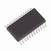
MAX395CWG+ Maxim Integrated Products, MAX395CWG+ Datasheet - Page 8

MAX395CWG+
Manufacturer Part Number
MAX395CWG+
Description
IC SWITCH OCTAL SPST 24SOIC
Manufacturer
Maxim Integrated Products
Datasheet
1.MAX395EWG.pdf
(16 pages)
Specifications of MAX395CWG+
Function
Switch
Circuit
8 x SPST - NO
On-state Resistance
175 Ohm
Voltage Supply Source
Single, Dual Supply
Voltage - Supply, Single/dual (±)
2.7 V ~ 16 V, ±2.7 V ~ 8 V
Current - Supply
7µA
Operating Temperature
0°C ~ 70°C
Mounting Type
Surface Mount
Package / Case
24-SOIC (0.300", 7.50mm Width)
Lead Free Status / RoHS Status
Lead free / RoHS Compliant
Serially Controlled, Low-Voltage,
8-Channel SPST Switch
TIMING CHARACTERISTICS—Single +3V Supply (Figure 1)
(V+ = +3.0V to +3.6V, V- = 0V, T
Note 1: The algebraic convention is used in this data sheet; the most negative value is shown in the minimum column.
Note 2: ∆R
Note 3: Leakage parameters are 100% tested at maximum rated hot temperature and guaranteed by correlation at room temp.
Note 4: Guaranteed by design.
Note 5: Leakage testing at single supply is guaranteed by testing with dual supplies.
Note 6: See Figure 6. Off isolation = 20log
Note 7: Between any two switches. See Figure 3.
8
SERIAL DIGITAL INTERFACE
SCLK Frequency
Cycle Time (Note 4)
CS Lead Time (Note 4)
CS Lag Time (Note 4)
SCLK High Time (Note 4)
SCLK Low Time (Note 4)
Data Setup Time (Note 4)
Data Hold Time (Note 4)
DIN Data Valid after Falling SCLK
(Note 4)
Rise Time of DOUT (Note 4)
Allowable Rise Time at DIN,
SCLK (Note 4)
Fall Time of DOUT (Note 4)
Allowable Fall Time at DIN,
SCLK (Note 4)
RESET Minimum Pulse Width
_______________________________________________________________________________________
specified voltages. Flatness is defined as the difference between the maximum and minimum value of on-resistance as
measured over the specified analog signal range.
PARAMETER
ON
= R
ON(max)
- R
ON(min)
A
= T
. On-resistance match between channels and on-resistance flatness are guaranteed only with
MIN
SYMBOL
t
CH
f
t
SCLK
t
CSH2
t
t
t
t
CSS
t
t
t
t
SCR
to T
t
t
SCF
CH
DH
DO
RW
CL
DS
DR
DF
+ t
10
CL
V
MAX
COM
, unless otherwise noted. Typical values are at T
/V
50% of SCLK to 10% of
DOUT, C
20% of V+ to 70% of V+,
C
20% of V+ to 70% of V+,
C
20% of V+ to 70% of V+,
C
20% of V+ to 70% of V+,
C
NO
L
L
L
L
= 10pF
= 10pF
= 10pF
= 10pF
, V
COM
L
= 10pF
= output. NO = input to off switch.
CONDITIONS
C, E, M
C, E, M
C, E, M
C, E, M
C, E, M
C, E, M
C, E, M
C, E, M
T
C, E, M
C, E, M
C, E, M
C, E, M
C, E, M
T
A
A
= +25°C
= +25°C
A
MIN
= +25°C.)
480
240
240
190
190
200
0
0
(Note 2)
TYP
150
105
-38
38
MAX
400
300
300
2.1
2
2
UNITS
MHz
ns
ns
ns
ns
ns
ns
ns
ns
ns
µs
ns
µs
ns


