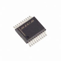
MAX4589CAP+ Maxim Integrated Products, MAX4589CAP+ Datasheet - Page 16

MAX4589CAP+
Manufacturer Part Number
MAX4589CAP+
Description
IC RF/VIDEO MUX DUAL 2CH 20-SSOP
Manufacturer
Maxim Integrated Products
Series
4000r
Datasheet
1.MAX4589EWP.pdf
(20 pages)
Specifications of MAX4589CAP+
Function
Video Multiplexer
Circuit
2 x 2:1
On-state Resistance
60 Ohm
Voltage Supply Source
Single, Dual Supply
Voltage - Supply, Single/dual (±)
2.7 V ~ 12 V, ± 2.7 V ~ 6 V
Operating Temperature
0°C ~ 70°C
Mounting Type
Surface Mount
Package / Case
20-SSOP
Lead Free Status / RoHS Status
Lead free / RoHS Compliant
Low-Voltage, High-Isolation,
Dual 2-Channel RF/Video Multiplexer
vias to connect the ground planes on each side of the
board. Logic-level signal routing is not critical.
The MAX4589 is intended for use in 75
where the inputs are terminated external to the IC and
the COM terminals are connected to an impedance of
600
75
However, variations in on-resistance and on-resistance
flatness cause nonlinearities.
The graphs shown in the Typical Operating Character-
istics for crosstalk and off-isolation are taken on adja-
cent channels. The adjacent channel is the worst-case
condition. For example, NO1 has the worst off-isolation
to COM1 due to its close proximity. Choosing channels
wisely necessitates separating the most sensitive chan-
nels from the most offensive. Conversely, the above
information also applies to the NO3 and NO4 inputs to
the COM2 pin.
The MAX4589 has internal circuitry to guarantee that all
switches are off on power-up (POR). This is equivalent
to the state resulting from asserting RS during normal
operation.
The serial mode is activated by driving the SER/PAR
input pin to a logic high. The data is then entered using
16
______________________________________________________________________________________
systems with terminations through the IC.
or higher. The MAX4589 operates in 50
Crosstalk and Off-Isolation
Power-On Reset (POR)
Impedance Matching
Serial Operation
systems,
and
a 4-bit SPI/MICROWIRE write operation. Systems that
must write longer data streams can ignore all but the
last four bits. Refer to Figure 7 for a detailed diagram of
the serial-interface logic. The first bit loaded is A0, then
A1, then an unused bit, followed by the disable bit.
There are four flip-flops in the input shift register. The
output of the 4th shift register is output on DOUT on the
rising edge of A1/SCLK. This allows cascading of multi-
ple MAX4589s using only one chip-select line. For
example, one 16-bit write programs the shift registers
of four cascaded MAX4589s. The data from the shift
register is moved to the internal control latches only
upon the rising edge of CS, so all four MAX4589s
change state simultaneously. RS has the same effect
as the internal power-on reset (POR) signal. The POR
state is A0 = A1 = 0 and disable = 1.
In serial mode, 2/4 is not used. Connect it to GND or
V
The parallel mode is activated by driving SER/PAR to a
logic low. The MAX4589 is then programmed by a
latched parallel bus scheme. Refer to Figure 6 for a
detailed diagram of the parallel-interface logic. If 2/4 is
high, A1 is disabled and the MAX4589 is configured as
a dual 1-of-2 multiplexer. If 2/4 is low, the MAX4589 is
configured as a 1-of-4 multiplexer. It is best to hard-wire
2/4 to a known state for the desired mode of operation,
or to use a dedicated microcontroller port pin.
L
; do not leave 2/4 unconnected.
Parallel Operation


