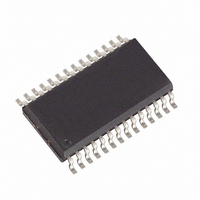
MAX4588CWI+ Maxim Integrated Products, MAX4588CWI+ Datasheet - Page 14

MAX4588CWI+
Manufacturer Part Number
MAX4588CWI+
Description
IC RF/VIDEO MUX DUAL 4CH 28-SOIC
Manufacturer
Maxim Integrated Products
Series
4000r
Datasheet
1.MAX4588CAI.pdf
(20 pages)
Specifications of MAX4588CWI+
Function
Video Multiplexer/Demultiplexer
Circuit
2 x 4:1
On-state Resistance
60 Ohm
Voltage Supply Source
Single, Dual Supply
Voltage - Supply, Single/dual (±)
2.7 V ~ 12 V, ± 2.7 V ~ 6 V
Operating Temperature
0°C ~ 70°C
Mounting Type
Surface Mount
Package / Case
28-SOIC (0.300", 7.50mm Width)
Lead Free Status / RoHS Status
Lead free / RoHS Compliant
The MAX4588 is optimized for ±5V operation. Using
lower supply voltages or a single supply increases
switching time, on-resistance (and therefore on-state
attenuation), and nonlinearity.
When the switch is off, MOSFETs N1, N2, P1, and P2
are off and MOSFET N3 is on (Figure 8). The signal
path is through the parasitic off-capacitances of the
series MOSFETs, but it is shunted to ground by N3.
This forms a highpass filter whose exact characteristics
are dependent on the source and load impedances. In
75Ω systems, and below 10MHz, the attenuation can
exceed 80dB. This value decreases with increasing fre-
quency and increasing circuit impedances. External
capacitance and board layout have a major role in
determining overall performance.
The MAX4588 construction is typical of many CMOS
analog switches. It has four supply pins: V+, V-, V
GND. V+ and V- are used to drive the internal CMOS
switches and set the limits of the analog voltage on any
switch. Reverse ESD-protection diodes are internally
connected between each analog signal pin and both
V+ and V-. If the voltage on any pin exceeds V+ or V-,
one of these diodes will conduct. During normal opera-
tion these reverse-biased ESD diodes leak, forming the
only current drawn from V- and V+.
Virtually all the analog leakage current is through the
ESD diodes. Although the ESD diodes on a given sig-
nal pin are identical, and therefore fairly well balanced,
they are reverse-biased differently. Each is biased by
either V+ or V- and the analog signal. This means their
leakages vary as the signal varies. The difference in the
two diode leakages from the signal path to the V+ and
V- pins constitutes the analog signal-path leakage cur-
rent. All analog leakage current flows to the supply ter-
minals, not to the other switch terminal. This explains
how both sides of a given switch can show leakage
currents of either the same or opposite polarity.
There is no connection between the analog signal
paths and GND. The analog signal paths consist of an
N-channel and P-channel MOSFET with their sources
and drains paralleled and their gates driven out of
phase with V+ and V- by the logic-level translators.
V
translators, and set the input logic thresholds. The
logic-level translators convert the logic levels to
switched V+ and V- signals to drive the gates of the
Low-Voltage, High-Isolation,
Dual 4-Channel RF/Video Multiplexer
14
L
and GND power the internal logic and logic-level
______________________________________________________________________________________
Applications Information
Power-Supply Considerations
Switch Off Condition
Overview
L
, and
analog switches. This drive signal is the only connec-
tion between the logic supplies and the analog sup-
plies.
The MAX4588 operates with bipolar supplies between
±2.7V and ±6V. The V+ and V- supplies are not required
to be symmetrical, but their sum cannot exceed the
absolute maximum rating of 13.0V. Do not connect the
MAX4588 V+ pin to +3V and connect the logic-level
input pins to +5V logic-level signals. This level
exceeds the absolute maximum ratings, and may
cause damage to the part and/or external circuits.
CAUTION: The absolute maximum V+ to V- differen-
tial voltage is 13.0V. Typical “±6-Volt” or “12-Volt”
supplies with ±10% tolerances can be as high as
13.2V. This voltage can damage the MAX4588. Even
±5% tolerance supplies may have overshoot or
noise spikes that exceed 13.0V.
The MAX4588 operates from a single supply between
+2.7V and +12V when V- is connected to GND.
Observe all of the precautions listed in the Bipolar-
Supply Operation section. Note, however, that these
parts are optimized for ±5V operation, and AC and DC
characteristics are degraded significantly when operat-
ing at less than ±5V. As the overall supply voltage (V+
to V-) is reduced, switching speed, on-resistance, off-
isolation, and distortion are degraded (see Typical
Operating Characteristics ).
Single-supply operation also limits signal levels and
interferes with grounded signals. When V- = 0, AC sig-
nals are limited to -0.3V. Voltages below -0.3V can be
clipped by the internal ESD-protection diodes, and the
parts can be damaged if excessive current flows.
When power to the MAX4588 is off (i.e., V+ = 0 and V-
= 0), the Absolute Maximum Ratings still apply. This
means that none of the MAX4588 pins can exceed
±0.3V. Voltages beyond ±0.3V cause the internal ESD-
protection diodes to conduct, with potentially cata-
strophic consequences.
When applying power to the MAX4588, follow this
sequence: V+, V- (if biased to potential other than
ground), V
analog NO_ and COM_ pins any time after V+, V-, and
GND voltages are set. Turning on all pins simultaneous-
ly is acceptable only if the circuit design guarantees
concurrent power-up.
L
, then logic inputs. Apply signals on the
Power-Supply Sequencing
Bipolar-Supply Operation
Single-Supply Operation
Power Off


