MAX4889AETO+T Maxim Integrated Products, MAX4889AETO+T Datasheet - Page 3
MAX4889AETO+T
Manufacturer Part Number
MAX4889AETO+T
Description
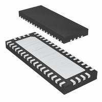
IC SWITCH OCTAL SPDT 42TQFN
Manufacturer
Maxim Integrated Products
Datasheet
1.MAX4888ETI.pdf
(14 pages)
Specifications of MAX4889AETO+T
Function
Switch
Circuit
8 x SPDT
On-state Resistance
7 Ohm
Voltage Supply Source
Single Supply
Voltage - Supply, Single/dual (±)
1.65 V ~ 3.6 V
Operating Temperature
-40°C ~ 85°C
Mounting Type
Surface Mount
Package / Case
42-WFQFN Exposed Pad
Lead Free Status / RoHS Status
Lead free / RoHS Compliant


ELECTRICAL CHARACTERISTICS (continued)
(V+ = +3.0V to +3.6V, T
Note 2: All units are 100% production tested at T
Note 3: ΔR
Note 4: Guaranteed by design. Not production tested.
Note 5: Flatness is defined as the difference between the maximum and minimum value of on-resistance as measured over the
DYNAMIC
Turn-On Time
Turn-Off Time
Propagation Delay
Output Skew Between Pairs
Output Skew Between Same
Pair
On-Loss
Crosstalk
Signaling Data Rate
Off-Isolation
NO_/NC_ Off-Capacitance
COM_ On-Capacitance
LOGIC INPUT
Input-Logic Low
Input-Logic High
Input-Logic Hysteresis
Input Leakage Current
POWER SUPPLY
Power-Supply Range
V+ Supply Current
Input Leakage Current
ESD PROTECTION
COM_+, COM_-
and characterization and are not production tested.
specified analog signal range.
PARAMETER
ON
= R
ON(MAX)
_______________________________________________________________________________________
A
5.0Gbps PCI Express Passive Switches
= -40°C to +85°C, unless otherwise noted. Typical values are at V+ = +3.3V, T
- R
ON(MIN)
C
C
NO_/NC_(OFF)
SYMBOL
COM_(ON)
.
V
G
V
V
t
t
t
t
HYST
t
BR
V
OFF
SK1
SK2
V
V+
I
I
ON
LOS
I+
PD
CT1
ISO
IN
IN
IH
IL
V
V
R
R
any two pairs, Figure 2
R
two lines on same pair, Figure 2
R
unbalanced,
Figure 3
Crosstalk between
any two pairs,
R
unbalanced,
Figure 3
R
Signal = 0dBm,
R
Figure 3
Figure 4
Figure 4
V
V
V
Human Body Model
A
NO_
NO_
SEL
SEL
SEL
S
S
S
S
S
S
S
= +85°C. Limits over the operating temperature range are guaranteed by design
= R
= R
= R
= R
= R
= R
= R
= 0V or V+
= 0V or V+
= 0V or V+
or V
or V
L
L
L
L
L
L
L
= 50 , unbalanced; skew between
= 50 , unbalanced; skew between
= 50 , unbalanced, Figure 2
= 50 ,
= 50 ,
= 50
= 50 ,
NC_
NC_
= +1.0V, R
= +1.0V, R
CONDITIONS
1MHz < f < 100MHz
500MHz < f < 1.25GHz
f = 50MHz
f = 1.25GHz
f = 10MHz
f = 1.25GHz
MAX4888A
MAX4889A
L
L
= 50 , Figure 1
= 50 , Figure 1
MIN
1.65
1.4
-1
-1
A
= +25°C.) (Note 2)
TYP
-0.5
-1.4
100
-53
-32
5.0
-56
-26
±6
90
10
50
50
10
1
2
MAX
3.60
250
120
0.5
+1
+1
50
60
UNITS
Gbps
mV
dB
dB
dB
μA
μA
μA
ns
ns
ps
ps
ps
pF
pF
kV
V
V
V
3
Related parts for MAX4889AETO+T
Image
Part Number
Description
Manufacturer
Datasheet
Request
R

Part Number:
Description:
MAX7528KCWPMaxim Integrated Products [CMOS Dual 8-Bit Buffered Multiplying DACs]
Manufacturer:
Maxim Integrated Products
Datasheet:
Part Number:
Description:
Single +5V, fully integrated, 1.25Gbps laser diode driver.
Manufacturer:
Maxim Integrated Products
Datasheet:
Part Number:
Description:
Single +5V, fully integrated, 155Mbps laser diode driver.
Manufacturer:
Maxim Integrated Products
Datasheet:
Part Number:
Description:
VRD11/VRD10, K8 Rev F 2/3/4-Phase PWM Controllers with Integrated Dual MOSFET Drivers
Manufacturer:
Maxim Integrated Products
Datasheet:
Part Number:
Description:
Highly Integrated Level 2 SMBus Battery Chargers
Manufacturer:
Maxim Integrated Products
Datasheet:
Part Number:
Description:
Current Monitor and Accumulator with Integrated Sense Resistor; ; Temperature Range: -40°C to +85°C
Manufacturer:
Maxim Integrated Products
Part Number:
Description:
TSSOP 14/A�/RS-485 Transceivers with Integrated 100O/120O Termination Resis
Manufacturer:
Maxim Integrated Products
Part Number:
Description:
TSSOP 14/A�/RS-485 Transceivers with Integrated 100O/120O Termination Resis
Manufacturer:
Maxim Integrated Products
Part Number:
Description:
QFN 16/A�/AC-DC and DC-DC Peak-Current-Mode Converters with Integrated Step
Manufacturer:
Maxim Integrated Products
Part Number:
Description:
TDFN/A/65V, 1A, 600KHZ, SYNCHRONOUS STEP-DOWN REGULATOR WITH INTEGRATED SWI
Manufacturer:
Maxim Integrated Products
Part Number:
Description:
Integrated Temperature Controller f
Manufacturer:
Maxim Integrated Products
Part Number:
Description:
SOT23-6/I�/45MHz to 650MHz, Integrated IF VCOs with Differential Output
Manufacturer:
Maxim Integrated Products
Part Number:
Description:
SOT23-6/I�/45MHz to 650MHz, Integrated IF VCOs with Differential Output
Manufacturer:
Maxim Integrated Products
Part Number:
Description:
EVALUATION KIT/2.4GHZ TO 2.5GHZ 802.11G/B RF TRANSCEIVER WITH INTEGRATED PA
Manufacturer:
Maxim Integrated Products
Part Number:
Description:
QFN/E/DUAL PCIE/SATA HIGH SPEED SWITCH WITH INTEGRATED BIAS RESISTOR
Manufacturer:
Maxim Integrated Products
Datasheet: