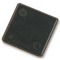
H5PS5162FFR-S6C HYNIX SEMICONDUCTOR, H5PS5162FFR-S6C Datasheet - Page 35

H5PS5162FFR-S6C
Manufacturer Part Number
H5PS5162FFR-S6C
Description
58T1896
Manufacturer
HYNIX SEMICONDUCTOR
Datasheet
1.H5PS5162FFR-S6C.pdf
(39 pages)
Specifications of H5PS5162FFR-S6C
Memory Type
SDRAM
Memory Configuration
32M X 16
Memory Case Style
FBGA
No. Of Pins
84
Operating Temperature Range
0°C To +85°C
Memory Size
512 Mbit
Voltage Vcc
1.8V
Rohs Compliant
Yes
Available stocks
Company
Part Number
Manufacturer
Quantity
Price
Company:
Part Number:
H5PS5162FFR-S6C
Manufacturer:
HYNIX
Quantity:
9 500
Company:
Part Number:
H5PS5162FFR-S6C
Manufacturer:
HYNIX
Quantity:
2 000
Company:
Part Number:
H5PS5162FFR-S6C
Manufacturer:
ST
Quantity:
40
Company:
Part Number:
H5PS5162FFR-S6C
Manufacturer:
HYNIX
Quantity:
4 000
Part Number:
H5PS5162FFR-S6C
Manufacturer:
HYNIX/海力士
Quantity:
20 000
Release
H5PS5162FFR series
28. If tDS or tDH is violated, data corruption may occur and the data must be re-written with valid data
before a valid READ can be executed.
29. These parameters are measured from a command/address signal (CKE, CS, RAS, CAS, WE, ODT, BA0,
A0, A1, etc.) transition edge to its respective clock signal (CK/CK) crossing. The spec values are not
affected by the amount of clock jitter applied (i.e. tJIT(per), tJIT(cc), etc.), as the setup and hold are rela-
tive to the clock signal crossing that latches the command/address. That is, these parameters should be
met whether clock jitter is present or not.
30. These parameters are measured from a data strobe signal ((L/U/R)DQS/DQS) crossing to its respective
clock signal (CK/CK) crossing. The spec values are not affected by the amount of clock jitter applied (i.e.
tJIT(per), tJIT(cc), etc.), as these are relative to the clock signal crossing. That is, these parameters should
be met whether clock jitter is present or not.
31. These parameters are measured from a data signal ((L/U) DM, (L/U) DQ0, (L/U) DQ1, etc.) transition
edge to its respective data strobe signal ((L/U/R)DQS/DQS) crossing.
32. For these parameters, the DDR2 SDRAM device is characterized and verified to support
tnPARAM = RU{tPARAM / tCK(avg)}, which is in clock cycles, assuming all input clock jitter specification-
sare satisfied.
For example, the device will support tnRP = RU {tRP / tCK(avg)}, which is in clock cycles, if all input clock
jitterspecifications are met. This means: For DDR2-667 5-5-5, of which tRP = 15ns, the device will support
tnRP =RU{tRP / tCK(avg)} = 5, i.e. as long as the input clock jitter specifications are met, Precharge com-
mand at Tm and Active command at Tm+5 is valid even if (Tm+5 - Tm) is less than 15ns due to input
clock jitter.
33. tDAL [nCK] = WR [nCK] + tnRP [nCK] = WR + RU {tRP [ps] / tCK(avg) [ps] }, where WR is the value
programmed in the mode register set.
34. New units, ‘tCK(avg)’ and ‘nCK’, are introduced in DDR2-667 and DDR2-800.
Unit ‘tCK(avg)’ represents the actual tCK(avg) of the input clock under operation.
Unit ‘nCK’, represents one clock cycle of the input clock, counting the actual clock edges.
Note that in DDR2-400 and DDR2-533, ‘tCK’, is used for both concepts.
ex) tXP = 2 [nCK] means; if Power Down exit is registered at Tm, an Active command may be registered
at Tm+2, even if (Tm+2 - Tm) is 2 x tCK(avg) + tERR(2per),min.
35. Input clock jitter spec parameter. These parameters and the ones in the table below are referred to as
'input clock jitter spec parameters' and these parameters apply to DDR2-667 and DDR2-800 only. The jitter
specified is a random jitter meeting a Gaussian distribution.
Rev. 1.0 / July. 2008
35


