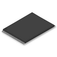
A43L0616BV-7F AMIC, A43L0616BV-7F Datasheet - Page 14

A43L0616BV-7F
Manufacturer Part Number
A43L0616BV-7F
Description
58T1324
Manufacturer
AMIC
Datasheet
1.A43L0616BV-7F.pdf
(48 pages)
Specifications of A43L0616BV-7F
Memory Type
SDRAM
Memory Configuration
1M X 16
Access Time
6ns
Interface Type
LVTTL
Memory Case Style
TSOPII
No. Of Pins
50
Operating Temperature Range
0°C To +70°C
Frequency
143MHz
Rohs Compliant
Yes
Available stocks
Company
Part Number
Manufacturer
Quantity
Price
Part Number:
A43L0616BV-7F
Manufacturer:
AMIC
Quantity:
20 000
Device Operations
Clock (CLK)
The clock input is used as the reference for all SDRAM
operations. All operations are synchronized to the positive
going edge of the clock. The clock transitions must be
monotonic between VIL and VIH. During operation with CKE
high all inputs are assumed to be in valid state (low or high)
for the duration of set up and hold time around positive edge
of the clock for proper functionality and ICC specifications.
Clock Enable (CKE)
The clock enable (CKE) gates the clock onto SDRAM. If CKE
goes low synchronously with clock (set-up and hold time
same as other inputs), the internal clock is suspended form
the next clock cycle and the state of output and burst address
is frozen as long as the CKE remains low. All other inputs are
ignored from the next clock cycle after CKE goes low. When
both banks are in the idle state and CKE goes low
synchronously with clock, the SDRAM enters the power down
mode form the next clock cycle. The SDRAM remains in the
power down mode ignoring the other inputs as long as CKE
remains low. The power down exit is synchronous as the
internal clock is suspended. When CKE goes high at least
“t
the SDRAM becomes active from the same clock edge
accepting all the input commands.
Bank Select (BA)
This SDRAM is organized as two independent banks of
524,288 words X 16 bits memory arrays. The BA inputs is
latched at the time of assertion of RAS and
the bank to be used for the operation. When BA is asserted
low, bank A is selected. When BA is asserted high, bank B is
selected. The bank select BA is latched at bank activate,
read, write mode register set and precharge operations.
Address Input (A0 ~ A10/AP)
The 19 address bits required to decode the 524,288 word
locations are multiplexed into 11 address input pins
(A0~A10/AP). The 11 bit row address is latched along with
column address is latched along with
during read or write command.
NOP and Device Deselect
When RAS ,
no operation (NOP). NOP does not initiate any new
operation, but is needed to complete operations which
require more than single clock like bank activate, burst read,
auto refresh, etc. The device deselect is also a NOP and is
entered by asserting CS high. CS
(February, 2008, Version 1.3)
RAS and BA during bank activate command. The 8 bit
SS
+ 1
CLOCK
CAS
” before the high going edge of the clock, then
and
WE
are high, the SDRAM performs
CAS
high disables the
CAS
,
WE
to select
and BA
13
command decoder so that RAS ,
address inputs are ignored.
Power-Up
The following sequence is recommended for POWER UP
1. Power must be applied to either CKE and DQM inputs to
2. After VDD reaches the desired voltage, a minimum pause
3. Both banks must be precharged now.
4. Perform a minimum of 2 Auto refresh cycles to stabilize the
5. Perform a MODE REGISTER SET cycle to program the
Mode Register Set (MRS)
The mode register stores the data for controlling the various
operation modes of SDRAM. It programs the CAS latency,
addressing mode, burst length, test mode and various vendor
specific options to make SDRAM useful for variety of different
applications. The default value of the mode register is not
defined, therefore the mode register must be written after
power up to operate the SDRAM. The mode register is
written by asserting low on CS , RAS ,
SDRAM should be in active mode with CKE already high
prior to writing the mode register). The state of address pins
A0~A10/AP
mode register. One clock cycle is required to complete the
write in the mode register. The mode register contents can
be changed using the same command and clock cycle
requirements during operation as long as both banks are in
the idle state. The mode register is divided into various fields
depending on functionality. The burst length field uses
A0~A2, burst type uses A3, addressing mode uses A4~A6,
A7~A8, A10/AP and BA are used for vendor specific options
or test mode. And the write burst length is programmed using
A9. A7~A8, A10/AP and BA must be set to low for normal
SDRAM operation.
Refer to table for specific codes for various burst length,
addressing modes and CAS latencies.
CS , RAS , CAS ,
pull them high and other pins are NOP condition at the
inputs before or along with VDD (and VDDQ) supply.
The clock signal must also be asserted at the same time.
of 200 microseconds is required with inputs in NOP
condition.
internal circuitry.
CAS latency, burst length and burst type as the default
value of mode register is undefined.
At the end of one clock cycle from the mode register set
cycle, the device is ready for operation.
When the above sequence is used for Power-up, all the
out-puts will be in high impedance state. The high
impedance of outputs is not guaranteed in any other
power-up sequence.
cf.) Sequence of 4 & 5 may be changed.
and
WE
BA
going low is the data written in the
AMIC Technology, Corp.
in
CAS
the
and
same
A43L0616B
CAS
WE
, and all the
cycle
,
WE
(The
as


