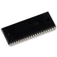
A42L0616V-50F AMIC, A42L0616V-50F Datasheet - Page 6

A42L0616V-50F
Manufacturer Part Number
A42L0616V-50F
Description
58T1323
Manufacturer
AMIC
Datasheet
1.A42L0616V-50F.pdf
(24 pages)
Specifications of A42L0616V-50F
Memory Type
DRAM
Memory Configuration
1M X 16
Access Time
50ns
Memory Case Style
TSOPII
No. Of Pins
44
Operating Temperature Range
0°C To +70°C
Ic Generic Number
42L0616
Memory Size
16Mbit
Rohs Compliant
Yes
Absolute Maximum Ratings*
Input Voltage (Vin) . . . . . . . . . . . . . . . . . . . . -0.5V to +4.6V
Output Voltage (Vout) . . . . . . . . . . . . . . . . . -0.5V to +4.6V
Power Supply Voltage (VCC) . . . . . . . . . . . -0.5V to +4.6V
Operating Temperature (T
Storage Temperature (T
Soldering Temperature X Time (T
. . . . . . . . . . . . . . . . . . . . . . . . . . . . . . . . . . 260 ° C X 10sec
Power Dissipation (P
Short Circuit Output Current (Iout) . . . . . . . . . . . . . . 50mA
Latch-up Current . . . . . . . . . . . . . . . . . . . . . . . . . . . 200mA
DC Electrical Characteristics
(July, 2004, Version 1.1)
Symbol
V
I
I
I
I
I
I
I
V
I
CC1
CC2
CC3
CC4
CC5
CC6
CC7
I
OL
IL
OH
OL
Input Leakage Current
Output Leakage Current
Operating Power Supply
Current
TTL Supply Current Supply
Current
Average Power Supply
Current, RAS Refresh
Mode
EDO Page Mode Average
Power Supply Current
Power Supply Current
CMOS Standby Power
Supply Current
Self Refresh Mode Current
Output Voltage
CAS -before- RAS Refresh
D
Parameter
) . . . . . . . . . . . . . . . . . . . . . . . . . 1W
STG
OPR
) . . . . . . . . . . -55 ° C to +150 ° C
) . . . . . . . . . . . 0 ° C to +70 ° C
SOLDER
(VCC = 3.3V ± 0.3V, VSS = 0V, Ta = 0 ° C to +70 ° C or -40 ° C to +85 ° C)
) . . . . . . . . . . . . . .
Min.
2.4
-5
-5
-
-
-
-
-
-
-
-
-45
Max.
110
110
110
110
1.5
1.0
1.0
0.4
+5
+5
-
Min.
2.4
-5
-5
5
-
-
-
-
-
-
-
-
*Comments
Stresses above those listed under "Absolute Maximum
Ratings" may cause permanent damage to this device.
These are stress ratings only. Functional operation of
this device at these or any other conditions above
those indicated in the operational sections of these
specification is not implied or intended. Exposure to
the absolute maximum rating conditions for extended
periods may affect device reliability.
-50
Max.
105
105
105
105
1.5
1.0
1.0
0.4
+5
+5
-
Unit
mA
mA
mA
mA
mA
mA
mA
µ A
µ A
V
V
Address cycling;
VCC - 0.2V
All other input high levels are
VCC-0.2V or input low levels
are VSS +0.2V
UCAS
UCAS
LCAS
RAS ,
RAS =
RAS and Address cycling,
RAS and address = V
RAS and
RAS =
RAS =
0V ≤ Vin ≤ Vin+0.3V
Pins not under
Test = 0V
D
0V ≤ Vout ≤ VCC
Address cycling;
t
t
t
t
I
I
RC
RC
PC
RC
OUT
OUT
OUT
AMIC Technology, Corp.
= min.
= min.
= min.
= min.
= -2.0mA
= 2.0mA
Test Conditions
UCAS
disabled,
UCAS
UCAS
CAS
=
,
cycling;
LCAS
LCAS
A42L0616 Series
UCAS
≤ VSS+0.2V
,
=
=
LCAS
LCAS
and
LCAS
= V
or
IH
,
and
= V
IL
=
,
IH
Notes
1, 2
1, 2
1
1


