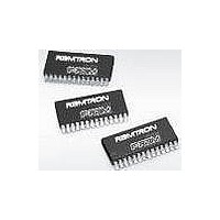
FM1608-120-S Ramtron, FM1608-120-S Datasheet - Page 4

FM1608-120-S
Manufacturer Part Number
FM1608-120-S
Description
F-RAM 64K (8Kx8) 120ns 5V
Manufacturer
Ramtron
Datasheet
1.FM1608-120-S.pdf
(12 pages)
Specifications of FM1608-120-S
Memory Size
64 KB
Organization
8 K x 8
Interface
Parallel
Access Time
120 ns
Operating Supply Voltage
0 V to + 5 V
Operating Temperature Range
- 40 C to + 85 C
Package / Case
SOIC-28
Mounting Style
SMD/SMT
Lead Free Status / Rohs Status
No
Available stocks
Company
Part Number
Manufacturer
Quantity
Price
Part Number:
FM1608-120-S
Manufacturer:
RAMTRON
Quantity:
20 000
Company:
Part Number:
FM1608-120-SG
Manufacturer:
RAMTRON
Quantity:
38 007
Company:
Part Number:
FM1608-120-SG
Manufacturer:
BAMTRON
Quantity:
3
Part Number:
FM1608-120-SG
Manufacturer:
RAMTRON
Quantity:
20 000
Company:
Part Number:
FM1608-120-SGTR
Manufacturer:
CYPRESS
Quantity:
5 000
Part Number:
FM1608-120-SGTR
Manufacturer:
RAMTRON
Quantity:
20 000
Unlike other truly nonvolatile memory technologies,
there is no write delay with F-RAM. Since the read
and write access times of the underlying memory are
the same, the user experiences no delay through the
bus. The entire memory operation occurs in a single
bus cycle. Therefore, any operation including read or
write can occur immediately following a write. Data
polling, a technique used with EEPROMs to
determine if a write is complete, is unnecessary.
Precharge Operation
The precharge operation is an internal condition that
prepares the memory for a new access. All memory
cycles consist of a memory access and a precharge.
The precharge is initiated by deasserting the /CE pin
high. It must remain high for at least the minimum
precharge time t
The user dictates the beginning of this operation since
a precharge will not begin until /CE rises. However
the device has a maximum /CE low time specification
that must be satisfied.
Endurance
The FM1608 internally operates with a read and
restore mechanism. Therefore, each read and write
cycle involves a change of state. The memory
architecture is based on an array of rows and
columns. Each read or write access causes an
endurance cycle for an entire row. In the FM1608, a
row is 32 bits wide. Every 4-byte boundary marks
the beginning of a new row. Endurance can be
optimized by ensuring frequently accessed data is
This product conforms to specifications per the terms of the Ramtron
standard warranty. The product has completed Ramtron’s internal
qualification testing and has reached production status.
Rev. 3.4
Nov. 2010
PC
.
located in different rows. Regardless, F-RAM offers
substantially higher write endurance than other
nonvolatile memories. The rated endurance limit of
10
same row for 10 years.
F-RAM Design Considerations
When designing with F-RAM for the first time, users
of SRAM will recognize a few minor differences.
First, bytewide F-RAM memories latch each address
on the falling edge of chip enable. This allows the
address bus to change after starting the memory
access. Since every access latches the memory
address on the falling edge of /CE, users cannot
ground it as they might with SRAM.
Users who are modifying existing designs to use F-
RAM should examine the memory controller for
timing compatibility of address and control pins.
Each memory access must be qualified with a low
transition of /CE. In many cases, this is the only
change
relationships is shown in Figure 2 below. Also shown
is a common SRAM signal relationship that will not
work for the FM1608.
The reason for /CE to strobe for each address is two-
fold: it latches the new address and creates the
necessary precharge period while /CE is high.
12
cycles will allow 3000 accesses per second to the
required.
1850 Ramtron Drive, Colorado Springs, CO 80921
An example
Ramtron International Corporation
(800) 545-FRAM, (719) 481-7000
http://www.ramtron.com
of the signal
FM1608
4 of 12


