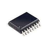
74LV4052PW NXP Semiconductors, 74LV4052PW Datasheet - Page 11

74LV4052PW
Manufacturer Part Number
74LV4052PW
Description
Multiplexer Switch ICs DUAL 4-CH MUX/DMUX
Manufacturer
NXP Semiconductors
Datasheet
1.74LV4052PW118.pdf
(16 pages)
Specifications of 74LV4052PW
Number Of Channels
2 Channel
On Resistance (max)
250 Ohms
Propagation Delay Time
25 ns, 9 ns, 6 ns, 5 ns, 4 ns, 3 ns
On Time (max)
190 ns
Off Time (max)
125 ns
Supply Voltage (max)
6 V
Supply Voltage (min)
1 V
Maximum Power Dissipation
400 mW
Maximum Operating Temperature
+ 125 C
Minimum Operating Temperature
- 40 C
Package / Case
TSSOP-16
Mounting Style
SMD/SMT
Number Of Lines (input / Output)
8 / 2
Lead Free Status / Rohs Status
Details
Other names
74LV4052PW,112
Available stocks
Company
Part Number
Manufacturer
Quantity
Price
Part Number:
74LV4052PW
Manufacturer:
NXP/恩智浦
Quantity:
20 000
Company:
Part Number:
74LV4052PW,118
Manufacturer:
NXP
Quantity:
150
Company:
Part Number:
74LV4052PWЈ¬118
Manufacturer:
NXP
Quantity:
7 500
1. V
2. V
3. V
Philips Semiconductors
WAVEFORMS
NOTES:
TEST CIRCUIT
1998 Jun 23
Dual 4-channel analog multiplexer/demultiplexer
V
the output load
V
V
V
Figure 13. Input (V
GENERATOR
M
M
OL
x
X
Y
Y
2.7 - 3.6V
= V
> 3.6 V
< 2.7V
= V
= V
= V
PULSE
= 1.5 V at 2.7 V
= 0.5
and V
OUTPUTS
V
OL
CC
OL
OH
OH
INPUTS
+ 0.3 V at 2.7 V
+ 0.1
V I
GND
V OH
– 0.3 V at 2.7 V
– 0.1
V OL
OH
V
CC
Test Circuit for Outputs
are the typical output voltage drop that occur with
2.7V
V
V
t PLH
V
at 2.7 V
CC
CC
V
I
V
l
V
CC
CC
R
T
is
V
at 2.7 V V
at 2.7 V V
) to output (V
CC
V M
V
t
t
t
PLH/
PLZ/
PHZ
V M
D.U.T.
CC
V
V
Test
V
3.6 V
cc
CC
CC
/t
t
t
PZL
PHL
PZH
3.6 V
CC
CC
3.6 V
3.6 V
os
V
O
3.6 V
) propagation delays.
3.6 V
2 V
C
Open
V
L
S
EE
1
CC
Figure 15. Load circuitry for switching times.
50 pF
SV01638
t PHL
Pulse
V
V
EE
V
IS
S
I
1
1kW
1kW
V
EE
2 V
Open
V
EE
CC
11
NEGATIVE
PULSE
POSITIVE
PULSE
R
C
R
pulse generators.
t
t
r
r
, t
L
L
T
90%
10%
=
f
= Load resistor
= Load capacitance includes jig and probe capacitance
= Termination resistance should be equal to Z
with 50% duty factor.
t
f
HIGH-to-OFF
OFF-to-HIGH
LOW-to-OFF
OFF-to-LOW
=6ns, when measuring f
OUTPUT
OUTPUT
INPUTS
V
V
for the inputs (S
M
GND
GND
10%
90%
M
V
Figure 14. Turn-on and turn-off times
V
V
V
OH
CC
OL
I
t
t
THL
TLH
(t
(t
f
enabled
)
outputs
r
)
V
DEFINITIONS
t
t
M
t
W
W
PLZ
t
PHZ
n
, E) to the output (V
V
10%
90%
max,
X
V
Y
V
there is no constraint on
V
M
M
disabled
outputs
90%
10%
t
PZL
t
t
t
PZH
TLH
THL
Product specification
74LV4052
OUT
(t
(t
V
r
f
os
0V
)
0V
)
V
V
M
V
SY01738
I
I
M
).
of
enabled
SV01640
outputs


