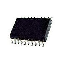
74HCT299D NXP Semiconductors, 74HCT299D Datasheet - Page 2

74HCT299D
Manufacturer Part Number
74HCT299D
Description
Counter Shift Registers 8-BIT UNIVERSAL SHFT REG 3-S
Manufacturer
NXP Semiconductors
Datasheet
1.74HCT299D.pdf
(11 pages)
Specifications of 74HCT299D
Counting Sequence
Serial/Parallel to Serial/Parallel
Number Of Circuits
1
Package / Case
SOT-163
Logic Family
HCT
Logic Type
CMOS
Output Type
3-State
Propagation Delay Time
37 ns
Supply Voltage (max)
5.5 V
Maximum Operating Temperature
+ 125 C
Minimum Operating Temperature
- 40 C
Function
Shift Register
Mounting Style
SMD/SMT
Operating Supply Voltage
5 V
Supply Voltage (min)
4.5 V
Lead Free Status / Rohs Status
Details
Other names
74HCT299D,652
Philips Semiconductors
FEATURES
GENERAL DESCRIPTION
The 74HC/HCT299 are high-speed Si-gate CMOS devices
and are pin compatible with low power Schottky TTL
(LSTTL). They are specified in compliance with JEDEC
standard no. 7A.
QUICK REFERENCE DATA
GND = 0 V; T
Notes
1. C
December 1990
SYMBOL
t
t
f
C
C
C
PHL/
PHL
max
Multiplexed inputs/outputs provide improved bit density
Four operating modes:
– shift left
– shift right
– hold (store)
– load data
Operates with output enable or at high-impedance
OFF-state (Z)
3-state outputs drive bus lines directly
Can be cascaded for n-bits word length
Output capability: bus driver (parallel I/Os),
standard (serial outputs)
I
8-bit universal shift register; 3-state
I
I/O
PD
CC
dissipation (P
f
f
C
V
i
o
CC
PD
= input frequency in MHz
L
t
category: MSI
= output frequency in MHz
(C
PLH
= output load capacitance in pF
P
= supply voltage in V
is used to determine the dynamic power
L
D
= C
V
amb
CC
PD
PARAMETER
propagation delay
maximum clock frequency
input capacitance
input/output capacitance
power dissipation capacitance per package
2
CP to Q
CP to I/O
MR to Q
= 25 C; t
D
V
in W):
f
o
CC
) = sum of outputs
2
0
0
, Q
n
, Q
f
r
i
= t
7
7
or I/O
f
= 6 ns
(C
L
n
V
CC
2
f
o
) where:
2
The 74HC/HCT299 contain eight edge-triggered D-type
flip-flops and the interstage logic necessary to perform
synchronous shift-right, shift-left, parallel load and hold
operations. The type of operation is determined by the
mode select inputs (S
select table.
All flip-flop outputs have 3-state buffers to separate these
outputs (I/O
inputs in the parallel load mode. The serial outputs (Q
Q
words.
A LOW signal on the asynchronous master reset input
(MR) overrides the S
flip-flops. All other state changes are initiated by the rising
edge of the clock pulse. Inputs can change when the clock
is either state, provided that the recommended set-up and
hold times, relative to the rising edge of CP, are observed.
A HIGH signal on the 3-state output enable inputs (OE
OE
set to the high-impedance OFF-state. In this condition, the
shift, hold, load and reset operations can still occur. The
3-state buffers are also disabled by HIGH signals on both
S
operation.
2. For HC the condition is V
ORDERING INFORMATION
See
Information”
0
7
) are used for expansion in serial shifting of longer
and S
2
For HCT the condition is V
) disables the 3-state buffers and the I/O
CONDITIONS
C
notes 1 and 2
“74HC/HCT/HCU/HCMOS Logic Package
L
= 15 pF; V
1
, when in preparation for a parallel load
0
.
to I/O
CC
7
) such, that they can serve as data
n
= 5 V
0
and clock (CP) inputs and resets the
and S
1
), as shown in the mode
I
I
= GND to V
= GND to V
74HC/HCT299
HC
20
20
20
50
3.5
10
120
Product specification
TYPICAL
HCT
19
19
23
46
3.5
10
125
CC
CC
n
outputs are
1.5 V
UNIT
ns
ns
ns
MHz
pF
pF
pF
0
and
1
or


