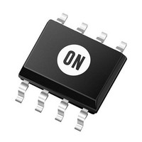
MC100ELT21D ON Semiconductor, MC100ELT21D Datasheet - Page 4

MC100ELT21D
Manufacturer Part Number
MC100ELT21D
Description
Translation - Voltage Levels 5V Diff PECL to TTL
Manufacturer
ON Semiconductor
Datasheet
1.MC10ELT21DTG.pdf
(8 pages)
Specifications of MC100ELT21D
Logic Type
Translator
Logic Family
ECL
Package / Case
SOIC-8
Translation
PECL to TTL
Propagation Delay Time
5.5 ns
Supply Voltage (max)
5.25 V
Supply Voltage (min)
4.75 V
Maximum Operating Temperature
+ 85 C
Minimum Operating Temperature
- 40 C
Mounting Style
SMD/SMT
Lead Free Status / Rohs Status
No RoHS Version Available
Available stocks
Company
Part Number
Manufacturer
Quantity
Price
Company:
Part Number:
MC100ELT21D
Manufacturer:
FUJITSU
Quantity:
2
Part Number:
MC100ELT21D
Manufacturer:
ON/安森美
Quantity:
20 000
Company:
Part Number:
MC100ELT21DG
Manufacturer:
ON Semiconductor
Quantity:
100
Company:
Part Number:
MC100ELT21DR2
Manufacturer:
MYSON
Quantity:
2 120
Company:
Part Number:
MC100ELT21DR2G
Manufacturer:
ON Semiconductor
Quantity:
2 500
Part Number:
MC100ELT21DT
Manufacturer:
ON
Quantity:
20 000
Company:
Part Number:
MC100ELT21DTG
Manufacturer:
ON Semiconductor
Quantity:
75
AC CHARACTERISTICS
NOTE: Device will meet the specifications after thermal equilibrium has been established when mounted in a test socket or printed circuit
8. R
9. V
Symbol
f
t
t
t
V
t
max
JITTER
PLH
PHL
r
/t
PP
f
PP
L
= 500 W to GND and C
board with maintained transverse airflow greater than 500 lfpm. Electrical parameters are guaranteed only over the declared
operating temperature range. Functional operation of the device exceeding these conditions is not implied. Device specification
limit values are applied individually under normal operating conditions and not valid simultaneously.
(min) is the minimum input swing for which AC parameters are guaranteed. The device has a DC gain of ≈ 40.
Maximum Toggle Frequency
Random Clock Jitter (RMS)
Propagation Delay @ 1.5 V
Propagation Delay @ 1.5 V
Input Swing (Note 9)
Output Rise/Fall Time
(10−90%)
Characteristic
V
L
CC
= 20 pF to GND. Refer to Figure 2.
Figure 2. TTL Output Loading Used for Device Evaluation
= 4.75 V to 5.25 V; GND = 0.0 V (Note 8)
*C
L
includes
fixture
capacitance
C
http://onsemi.com
L
Min
200
*
2.0
2.0
CHARACTERISTIC TEST
GND
−40°C
APPLICATION
Typ
4
R
1000
Max
L
5.5
5.5
TTL RECEIVER
Min
200
2.0
2.0
AC TEST LOAD
25°C
Typ
100
750
35
1000
Max
5.5
5.5
Min
200
2.0
2.0
85°C
Typ
1000
Max
5.5
5.5
MHz
Unit
mV
ps
ns
ns
ps


