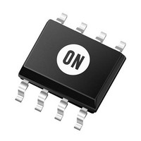
MC100EPT24D ON Semiconductor, MC100EPT24D Datasheet

MC100EPT24D
Specifications of MC100EPT24D
Available stocks
Related parts for MC100EPT24D
MC100EPT24D Summary of contents
Page 1
MC100EPT24 3.3V LVTTL/LVCMOS to Differential LVECL Translator Description The MC100EPT24 is a LVTTL/LVCMOS to differential LVECL translator. Because LVECL levels and LVTTL/LVCMOS levels are used, a −3.3 V, +3.3 V and ground are required. The small outline 8−lead package and the ...
Page 2
LVTTL D 2 LVECL Figure 1. 8−Lead Pinout (Top View) and Logic Diagram Table 2. ATTRIBUTES Characteristics Internal Input Pulldown Resistor Internal Input Pullup Resistor ESD Protection Moisture Sensitivity, Indefinite Time Out of ...
Page 3
Table 3. MAXIMUM RATINGS Symbol Parameter V Positive Power Supply CC V Negative Power Supply EE V Input Voltage IN I Output Current out T Operating Temperature Range A T Storage Temperature Range stg Thermal Resistance (Junction−to−Ambient ...
Page 4
Table 6. AC CHARACTERISTICS V Symbol Characteristic f Maximum Input Clock Frequency (Fig- max ure Propagation Delay to PLH t Output Differential (Note 6) PHL t RMS Random Clock Jitter (Figure 2) JITTER t Output Rise/Fall Times ...
Page 5
... ORDERING INFORMATION Device MC100EPT24D MC100EPT24DG MC100EPT24DR2 MC100EPT24DR2G MC100EPT24DT MC100EPT24DTG MC100EPT24DTR2 MC100EPT24DTR2G MC100EPT24MNR4 MC100EPT24MNR4G †For information on tape and reel specifications, including part orientation and tape sizes, please refer to our Tape and Reel Packaging Specifications Brochure, BRD8011/D. Resource Reference of Application Notes AN1405/D AN1406/D ...
Page 6
... G C SEATING PLANE −Z− 0.25 (0.010 *For additional information on our Pb−Free strategy and soldering details, please download the ON Semiconductor Soldering and Mounting Techniques Reference Manual, SOLDERRM/D. PACKAGE DIMENSIONS SOIC−8 NB CASE 751−07 ISSUE 0.10 (0.004 SOLDERING FOOTPRINT* 1 ...
Page 7
K 8x REF 0.10 (0.004) 0.15 (0.006 L −U− PIN 1 IDENT 0.15 (0.006 −V− C 0.10 (0.004) D −T− G SEATING PLANE PACKAGE DIMENSIONS TSSOP−8 ...
Page 8
... Opportunity/Affirmative Action Employer. This literature is subject to all applicable copyright laws and is not for resale in any manner. PUBLICATION ORDERING INFORMATION LITERATURE FULFILLMENT: Literature Distribution Center for ON Semiconductor P.O. Box 5163, Denver, Colorado 80217 USA Phone: 303−675−2175 or 800−344−3860 Toll Free USA/Canada Fax: 303− ...


