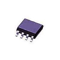
CAT93C66S Catalyst / ON Semiconductor, CAT93C66S Datasheet - Page 8

CAT93C66S
Manufacturer Part Number
CAT93C66S
Description
EEPROM (512x8) (256x16) 4K
Manufacturer
Catalyst / ON Semiconductor
Specifications of CAT93C66S
Memory Size
4 Kbit
Organization
512 K x 8 or 256 K x 16
Interface Type
Microwire
Maximum Clock Frequency
1 MHz
Supply Voltage (max)
6 V
Supply Voltage (min)
2.5 V
Maximum Operating Current
3 mA
Maximum Operating Temperature
+ 70 C
Mounting Style
SMD/SMT
Package / Case
SOIC-8
Minimum Operating Temperature
0 C
Operating Supply Voltage
2.5 V, 6 V
Operating Temperature
0 C to + 70 C
Lead Free Status / Rohs Status
No
Available stocks
Company
Part Number
Manufacturer
Quantity
Price
Company:
Part Number:
CAT93C66S
Manufacturer:
CATALYST
Quantity:
1 490
Part Number:
CAT93C66S
Manufacturer:
CSI
Quantity:
20 000
Company:
Part Number:
CAT93C66S-26490T13
Manufacturer:
CAT
Quantity:
1 925
Part Number:
CAT93C66S-26490T13
Manufacturer:
CATALYST
Quantity:
20 000
Part Number:
CAT93C66S-26627T
Manufacturer:
CSI
Quantity:
20 000
Company:
Part Number:
CAT93C66S-TE13
Manufacturer:
MICRONAS
Quantity:
37
Company:
Part Number:
CAT93C66SA-26547T
Manufacturer:
CATALYST
Quantity:
6 000
Part Number:
CAT93C66SA-26547T
Manufacturer:
CATALYST
Quantity:
20 000
Part Number:
CAT93C66SA-547-TE13
Manufacturer:
CATALYST
Quantity:
20 000
Erase
Upon receiving an ERASE command and address, the
CS (Chip Select) pin must be deasserted for a minimum
of t
clear cycle of the selected memory location. The clocking
of the SK pin is not necessary after the device has
entered the self clocking mode. The ready/busy status of
the CAT93C46/56/57/66/86 can be determined by
selecting the device and polling the DO pin. Once
cleared, the content of a cleared location returns to a
logical “1” state.
Erase/Write Enable and Disable
The CAT93C46/56/57/66/86 powers up in the write
disable state. Any writing after power-up or after an
EWDS (write disable) instruction must first be preceded
by the EWEN (write enable) instruction. Once the write
instruction is enabled, it will remain enabled until power
to the device is removed, or the EWDS instruction is
sent. The EWDS instruction can be used to disable all
CAT93C46/56/57/66/86 write and clear instructions,
and will prevent any accidental writing or clearing of the
device. Data can be read normally from the device
regardless of the write enable/disable status.
Figure 4. Erase Instruction Timing
93C46/56/57/66/86
Doc. No. 1023, Rev. J
DO
CS
SK
DI
CSMIN
. The falling edge of CS will start the self clocking
1
1
1
A N
A N-1
HIGH-Z
8
A 0
Erase All
Upon receiving an ERAL command, the CS (Chip Select)
pin must be deselected for a minimum of t
falling edge of CS will start the self clocking clear cycle
of all memory locations in the device. The clocking of the
SK pin is not necessary after the device has entered the
self clocking mode. The ready/busy status of the
CAT93C46/56/57/66/86 can be determined by selecting
the device and polling the DO pin. Once cleared, the
contents of all memory bits return to a logical “1” state.
Write All
Upon receiving a WRAL command and data, the CS
(Chip Select) pin must be deselected for a minimum of
t
data write to all memory locations in the device. The
clocking of the SK pin is not necessary after the device
has entered the self clocking mode. (Note 1.) The ready/
busy status of the CAT93C46/56/57/66/86 can be
determined by selecting the device and polling the DO
pin. It is not necessary for all memory locations to be
cleared before the WRAL command is executed.
CSMIN
. The falling edge of CS will start the self clocking
t SV
t EW
STATUS VERIFY
t CS
BUSY
READY
STANDBY
t HZ
HIGH-Z
93C46/56/57/66/86 F06
CSMIN
. The


