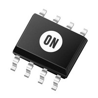
MC34072D ON Semiconductor, MC34072D Datasheet - Page 2

MC34072D
Manufacturer Part Number
MC34072D
Description
Op Amps 3-44V Dual 5mV VIO
Manufacturer
ON Semiconductor
Datasheet
1.MC33072ADG.pdf
(25 pages)
Specifications of MC34072D
Number Of Channels
2
Voltage Gain Db
100 dB
Common Mode Rejection Ratio (min)
70 dB
Input Voltage Range (max)
Positive Rail - 1.8 V
Input Voltage Range (min)
Negative Rail
Input Offset Voltage
5 mV
Operating Supply Voltage
44 V
Supply Current
3.8 mA
Maximum Operating Temperature
+ 70 C
Mounting Style
SMD/SMT
Package / Case
SOIC-8
Maximum Dual Supply Voltage
+/- 22 V
Minimum Operating Temperature
0 C
Lead Free Status / Rohs Status
No
Available stocks
Company
Part Number
Manufacturer
Quantity
Price
Part Number:
MC34072D
Manufacturer:
ON/安森美
Quantity:
20 000
Part Number:
MC34072DR
Manufacturer:
ON/安森美
Quantity:
20 000
Part Number:
MC34072DR2
Manufacturer:
ON/安森美
Quantity:
20 000
Company:
Part Number:
MC34072DR2G
Manufacturer:
OMRON
Quantity:
10 000
Company:
Part Number:
MC34072DR2G
Manufacturer:
ON
Quantity:
100 000
Company:
Part Number:
MC34072DR2G
Manufacturer:
ON75
Quantity:
2 500
Part Number:
MC34072DR2G
Manufacturer:
ON/安森美
Quantity:
20 000
Stresses exceeding Maximum Ratings may damage the device. Maximum Ratings are stress ratings only. Functional operation above the
Recommended Operating Conditions is not implied. Extended exposure to stresses above the Recommended Operating Conditions may affect
device reliability.
1. Either or both input voltages should not exceed the magnitude of V
2. Power dissipation must be considered to ensure maximum junction temperature (T
MAXIMUM RATINGS
Supply Voltage (from V
Input Differential Voltage Range
Input Voltage Range
Output Short Circuit Duration (Note 2)
Operating Junction Temperature
Storage Temperature Range
Offset Null
Inputs
Inputs 1
Output 1
Inputs
CASE 626/CASE 751
V
V
EE
EE
-
+
1
2
3
4
(Single, Top View)
(Dual, Top View)
2
3
4
1
+
-
-
+
Q1
Bias
EE
-
+
Q2
8
7
6
5
to V
8
7
6
5
Output 2
V
NC
V
Output
Offset Null
CC
CC
Inputs 2
CC
Rating
Q3
Q8
)
Cancellation
Current
Base
(MC33071, MC34071 only)
Figure 1. Representative Schematic Diagram
Offset Null
R1
Inputs 1
Inputs 2
Output 1
Q4
Output 2
Q9
CASE 646/CASE 751A/CASE 948G
V
R3
Q12
D1
CC
C1
1
2
3
4
5
6
7
PIN CONNECTIONS
Q10
http://onsemi.com
(Quad, Top View)
+
-
-
+
Q13
(Each Amplifier)
R2
R4
2
1
3
4
2
CC
Q5
-
+
+
-
or V
14
13
12
11
10
9
8
Q11
Output 4
V
Output 3
EE
EE
Q14
Symbol
Inputs 4
Inputs 3
.
V
T
V
t
V
T
SC
IDR
stg
IR
S
J
Q6
J
) is not exceeded (see Figure 2).
C2
Q15
Output 1
Q7
R5
In + 1
In 1
D2
NC
Q16
Q17
−60 to +150
Indefinite
D3
(Note 1)
(Note 1)
2
3
4
R6
Value
1
+150
+44
CASE 510AJ
R7
(Top View)
VEE/GND
Current
VCC
10
Q18
Q19
5
Limit
R8
V
EE
V
/GND
CC
Output
9
8
7
6
Unit
Sec
°C
°C
V
V
V
Output 2
NC
In 2
In + 2


