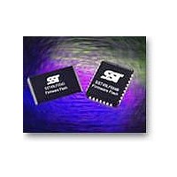
SST49LF004B-33-4C-NH Microchip Technology, SST49LF004B-33-4C-NH Datasheet - Page 15

SST49LF004B-33-4C-NH
Manufacturer Part Number
SST49LF004B-33-4C-NH
Description
Flash 512K X 8 33ns
Manufacturer
Microchip Technology
Datasheet
1.SST49LF004B-33-4C-NH.pdf
(36 pages)
Specifications of SST49LF004B-33-4C-NH
Data Bus Width
8 bit
Memory Type
NAND
Memory Size
4 Mbit
Architecture
Sectored
Interface Type
LPC
Access Time
33 ns
Supply Voltage (max)
3.6 V
Supply Voltage (min)
3 V
Maximum Operating Current
12 mA
Operating Temperature
+ 70 C
Mounting Style
SMD/SMT
Package / Case
PLCC-32
Organization
512 KB x 8
Lead Free Status / Rohs Status
No
Available stocks
Company
Part Number
Manufacturer
Quantity
Price
Company:
Part Number:
SST49LF004B-33-4C-NH
Manufacturer:
SST
Quantity:
5 530
Company:
Part Number:
SST49LF004B-33-4C-NH
Manufacturer:
SST
Quantity:
5 120
Part Number:
SST49LF004B-33-4C-NH
Manufacturer:
SST
Quantity:
20 000
Company:
Part Number:
SST49LF004B-33-4C-NHE
Manufacturer:
SST
Quantity:
5 530
Company:
Part Number:
SST49LF004B-33-4C-NHE
Manufacturer:
SST
Quantity:
5 120
Company:
Part Number:
SST49LF004B-33-4C-NHE
Manufacturer:
SST
Quantity:
48
Part Number:
SST49LF004B-33-4C-NHE
Manufacturer:
SST
Quantity:
20 000
4 Mbit Firmware Hub
SST49LF004B
Write Operation Status Detection
The SST49LF004B device provides two software means to
detect the completion of a Write (Program or Erase) cycle,
in order to optimize the system Write cycle time. The soft-
ware detection includes two status bits: Data# Polling, DQ
and Toggle Bit, DQ
incorporated into the Firmware Memory Read cycles. The
actual completion of the nonvolatile write is asynchronous
with the system. Therefore, either a Data# Polling or Toggle
Bit read may be simultaneous with the completion of the
Write cycle. If this occurs, the system may possibly get an
erroneous result, i.e., valid data may appear to conflict with
either DQ
an erroneous result occurs, the software routine should
include a loop to read the accessed location an additional
two (2) times. If both reads are valid, then the device has
completed the Write cycle, otherwise the rejection is valid.
Data# Polling
When the SST49LF004B device is in the internal Program
operation, any attempt to read DQ
plement of the true data. Once the Program operation is
completed, DQ
though DQ
completion of an internal Write operation, the remaining
data outputs may still be invalid. Valid data will appear on
the entire data bus in subsequent successive Read cycles
after an interval of 1 µs. During an internal Erase operation,
any attempt to read DQ
nal Erase operation is completed, DQ
Proper status will not be given using Data# Polling if the
address is in the invalid range.
Toggle Bit
During the internal Program or Erase operation, any consec-
utive attempts to read DQ
1s, i.e., toggling between 0 and 1. When the internal Pro-
gram or Erase operation is completed, the toggling will stop.
Note that even though DQ
following the completion of an internal Write operation, the
remaining data outputs may still be invalid. Valid data will
appear on the entire data bus in subsequent successive
Read cycles after an interval of 1 µs. Proper status will not be
given using Toggle Bit if the address is in the invalid range.
©2007 Silicon Storage Technology, Inc.
7
7
or DQ
may have valid data immediately following the
7
6.
will produce true data. Note that even
In order to prevent spurious rejection, if
6.
The End-of-Write detection mode is
7
will produce a '0'. Once the inter-
6
6
may have valid data immediately
will produce alternating 0s and
7
will produce the com-
7
will produce a '1'.
7,
15
Registers
There are three types of registers available on the
SST49LF004B, the General Purpose Inputs register, Block
Locking registers, and the JEDEC ID registers. These reg-
isters appear at their respective address location in the 4
GByte system memory map. Unused register locations will
read as 00H. Any attempt to read or write any register dur-
ing an internal Write operation will be ignored.
General Purpose Inputs Register
The GPI_REG (General Purpose Inputs Register) passes
the state of GPI[4:0] to the outputs. It is recommended that
the GPI[4:0] pins are in the desired state before LFRAME#
is brought low for the beginning of the bus cycle, and remain
in that state until the end of the cycle. There is no default
value since this is a pass-through register. The GPI register
for the boot device appears at FFBC0100H in the 4 GByte
system memory map, and will appear elsewhere if the
device is not the boot device. The register is not available to
be read when the device is in Erase/Program operation.
Block Locking Registers
SST49LF004B provides software controlled lock protection
through a set of Block Locking registers. The Block Locking
registers are Read/Write registers and are accessible
through standard addressable memory locations specified
in Table 7 for boot device. These registers will appear else-
where if the device is not the boot device. Unused register
locations will read as 00H.
Write Lock: The Write-Lock bit, bit 0, controls the lock
state. The default Write status of all blocks after power up is
write locked. When bit 0 of the Block Locking register is set,
Program and Erase operations for the corresponding block
are prevented. Clearing the Write-Lock bit will unprotect the
block. The Write-Lock bit must be cleared prior to starting a
Program or Erase operation since it is sampled at the
beginning of the operation.
The Write-Lock bit functions in conjunction with the hard-
ware Write Lock pin TBL# for the top Boot Block. When
TBL# is low, it overrides the software locking scheme. The
top Boot Block Locking register does not indicate the state
of the TBL# pin.
The Write-Lock bit functions in conjunction with the hard-
ware WP# pin for blocks 0 to 6. When WP# is low, it over-
rides the software locking scheme. The Block Locking
registers do not indicate the state of the WP# pin.
S71307-03-EOL
EOL Data Sheet
12/07


