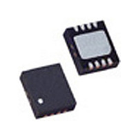
LT5537EDDB#PBF Linear Technology, LT5537EDDB#PBF Datasheet - Page 9

LT5537EDDB#PBF
Manufacturer Part Number
LT5537EDDB#PBF
Description
Manufacturer
Linear Technology
Datasheet
1.LT5537EDDBPBF.pdf
(16 pages)
Specifications of LT5537EDDB#PBF
Pin Count
8
Screening Level
Industrial
Package Type
DFN
Lead Free Status / Rohs Status
Compliant
Available stocks
Company
Part Number
Manufacturer
Quantity
Price
APPLICATIO S I FOR ATIO
Dynamic Range
The LT5537 is capable of detecting and log-converting an
input signal over a wide dynamic range. The range of the
output voltage may be limited, however, and the monoto-
nicity of the output versus input at high input level may be
affected if the supply voltage is low and the log-linear slope
is set too high. The minimum V
dynamic range with 20mV/dB slope is 2.8V under nominal
conditions at 25°C. The data shown in the Typical Perfor-
mance Characteristics plots was taken with V
there is difficulty encountered in achieving the desired
dynamic range, then the user is advised to increase the
supply voltage or else to decrease the output slope by
connecting a smaller valued resistor between the output
and ground.
IN
IN
+
–
CAP
Figure 3. Simplified Input Circuit
+
7k
V
CAP
Figure 4. Input Admittance
CC
U
–
7k
V
BIAS
U
5537 F04
W
CC
to support 90dB
TO 2ND
STAGE
U
CC
= 3V. If
Input Matching
The LT5537 has a high impedance input (Figure 3). The
differential input impedance is derived from S11 measure-
ment with one of the input pins AC grounded (Figure 4). At
200MHz, the input is equivalent to 1.73k//1.45pF (Table 1).
The input dynamic range is constant in voltage terms,
ranging from approximately –89dBVrms to 1dBVrms at
200MHz. The dynamic range expressed in power is
dependent on the actual impedance selected in the ap-
plication design.
Table 1. Parallel Equivalent RC of the LT5537 Input
The simplest way of input matching the LT5537 is to
terminate the input signal with a 50Ω resistor and AC
couple it to one of the input pins while AC grounding the
other input pin (Figure 13). The sensitivity (defined as the
minimum input power required for the output to be within
3dB of the ideal log-linear response) is –76.4dBm at
200MHz in this case.
To achieve the best sensitivity, the input termination
impedance should be increased and the input pins should
be differentially driven. An example application circuit is
shown in Figure 5 which uses a transformer to step up the
impedance and perform the balun function. The 240Ω
resistor (R2) sets the impedance at the input of the chip to
200Ω. A 1:4 transformer is used to match the 50Ω signal
source impedance to the circuit input impedance. C1 and
C2 are DC blocking capacitors. This application circuit has
a (3dB error) sensitivity of –82.4dBm at 200MHz.
FREQUENCY
1000MHz
100MHz
200MHz
400MHz
600MHz
800MHz
Figure 5. Differential Input Matching to 200Ω
INPUT
J1
M/A-COM
ETC4-1-2
(1:4)
1.85kΩ
1.73kΩ
1.07kΩ
673Ω
435Ω
303Ω
R
N/C
R2
240Ω
C1
C2
5537 F06
LT5537
1.51pF
1.45pF
1.48pF
1.52pF
1.65pF
1.78pF
IN
IN
2
3
C
+
–
5537fa
9


