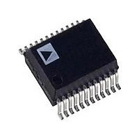
AD7011ARS Analog Devices Inc, AD7011ARS Datasheet - Page 4

AD7011ARS
Manufacturer Part Number
AD7011ARS
Description
Manufacturer
Analog Devices Inc
Datasheet
1.AD7011ARS.pdf
(12 pages)
Specifications of AD7011ARS
Device Type
Modulator
Modulation Type
Quadrature
Pin Count
24
Package Type
SSOP
Lead Free Status / Rohs Status
Not Compliant
Available stocks
Company
Part Number
Manufacturer
Quantity
Price
Part Number:
AD7011ARS
Manufacturer:
ADI/亚德诺
Quantity:
20 000
Part Number:
AD7011ARSZ
Manufacturer:
ADI/亚德诺
Quantity:
20 000
AD7011
TRANSMIT SECTION TIMING
Parameter
t
t
t
t
t
t
t
t
t
t
t
t
t
t
t
t
4
5
6
7
8
9
10
11
12
13
14
15
16
17
18
19
POWER
TxDATA
READY
TxCLK
MCLK
BIN
Limit at T
10
t
4097t
10
t
t
3t
64t
32t
32t
50
0
3t
124t
7.5t
30t
10
10
1
1
1
TxDATA
1
1
POWER
– 10
– 10
+ 70
READY
TxCLK
MCLK
1
1
1
1
+ 70
9
1
BIN
1
+ 70
t
14
t
4
A
= –40 C to +85 C
X
t
N+4
5
Figure 4. Transmit Timing at the Start of a Tx Burst
Figure 5. Transmit Timing at the End of a Tx Burst
t
(V
T
15
MIN
AA
= V
to T
DD
MAX
t
7
= +5 V
unless otherwise noted.)
t
Y
6
Units
ns min
ns max
ns max
ns min
ns max
ns max
ns
ns
ns
ns
ns min
ns min
ns max
ns max
ns
ns max
ns max
ns max
N+4
t
8
10%; AGND = DGND = 0 V, f
–4–
Description
TxCLK Cycle Time.
TxCLK High Time.
TxCLK Low Time.
Ramp Down cycle time after the last transmitted symbol.
Power Setup Time.
MCLK rising edge, after Power high, to READY rising edge.
BIN Setup Time.
MCLK to READY propagation delay.
MCLK rising edge, after BIN high, to first TxCLK rising edge.
TxCLK falling edge to TxDATA setup time.
TxCLK falling edge to TxDATA hold time.
BIN low setup to Last transmitted symbol after ramp down.
BIN low hold to Last transmitted symbol after ramp down.
Last TxCLK falling edge to READY rising edge.
Digital Output Rise Time.
Digital Output Fall Time.
X
N+5
t
12
t
X
9
k
t
13
t
11
MCLK
t
16
= 3.1104 MHz. All specifications are
X
N+8
t
10
Y
k
Y
N+8
t
17
REV. B


