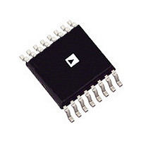
AD7811YRU-REEL Analog Devices Inc, AD7811YRU-REEL Datasheet - Page 3

AD7811YRU-REEL
Manufacturer Part Number
AD7811YRU-REEL
Description
Manufacturer
Analog Devices Inc
Datasheet
1.AD7811YRU-REEL.pdf
(19 pages)
Specifications of AD7811YRU-REEL
Number Of Elements
1
Resolution
10Bit
Architecture
SAR
Sample Rate
350KSPS
Input Polarity
Unipolar
Input Type
Voltage
Rated Input Volt
2.5/5V
Differential Input
Yes
Power Supply Requirement
Single
Single Supply Voltage (typ)
3.3/5V
Single Supply Voltage (min)
2.7V
Single Supply Voltage (max)
5.5V
Dual Supply Voltage (typ)
Not RequiredV
Dual Supply Voltage (min)
Not RequiredV
Dual Supply Voltage (max)
Not RequiredV
Power Dissipation
10.5mW
Differential Linearity Error
±1LSB
Integral Nonlinearity Error
±1LSB
Operating Temp Range
-40C to 105C
Operating Temperature Classification
Industrial
Mounting
Surface Mount
Pin Count
16
Package Type
TSSOP
Lead Free Status / Rohs Status
Not Compliant
Available stocks
Company
Part Number
Manufacturer
Quantity
Price
Company:
Part Number:
AD7811YRU-REEL
Manufacturer:
AD
Quantity:
3 753
Parameter
POWER SUPPLY
NOTES
1
2
Specifications subject to change without notice.
TIMING CHARACTERISTICS
Parameter
t
t
t
t
t
t
t
t
t
t
t
t
NOTES
1
2
3
4
Specifications subject to change without notice.
See Terminology.
Sample tested during initial release and after any redesign or process change that may affect this parameter.
POWER-UP
5
6
7
10
11
Sample tested to ensure compliance.
See Figures 16, 17 and 18.
These numbers are measured with the load circuit of Figure 1. They are defined as the time required for the o/p to cross 0.8 V or 2.4 V for V
0.4 V or 2 V for V
Derived from the measured time taken by the data outputs to change 0.5 V when loaded with the circuit of Figure 1. The measured number is then extrapolated back
to remove the effects of charging or discharging the 50 pF capacitor. This means that the time, t
time of the part and as such is independent of external bus loading capacitances.
1
2
3
4
8
9
3
3
3
V
I
Power Dissipation
3, 4
DD
DD
Normal Operation
Power-Down
Full Power-Down
Partial Power-Down (Internal Ref)
Normal Operation
Auto Full Power-Down
Partial Power-Down (Internal Ref)
Full Power-Down
Throughput 1 kSPS
Throughput 10 kSPS
Throughput 100 kSPS
DD
= 3 V ± 10%.
Y Version
1.5
2.3
20
25
25
5
5
10
10
5
20
100
Unit
µs (max)
µs (max)
ns (min)
ns (min)
ns (min)
ns (min)
ns (min)
ns (max)
ns (min)
ns (min)
ns (max)
ns (min)
1, 2
(V
OUTPUT
DD
Y Version
2.7
5.5
3.5
1
350
10.5
31.5
315
3.15
1.05
3
= 2.7 V to 5.5 V, V
PIN
TO
50pF
C
Conditions/Comments
Power-Up Time of AD7811/AD7812 after Rising Edge of CONVST
Conversion Time
CONVST Pulsewidth
SCLK High Pulsewidth
SCLK Low Pulsewidth
RFS Rising Edge to SCLK Rising Edge Setup Time
TFS Falling Edge to SCLK Falling Edge Setup Time
SCLK Rising Edge to Data Out Valid
DIN Data Valid to SCLK Falling Edge Setup Time
DIN Data Valid after SCLK Falling Edge Hold Time
SCLK Rising Edge to D
DOUT High Impedance to CONVST Falling Edge
L
200 A
V min
V max
mA max
µA max
µA max
mW max
µW max
µW max
mW max
mW max
µW max
200 A
Unit
REF
= V
DD
I
I
[EXT] unless otherwise noted)
OL
OH
11
, quoted in the Timing Characteristics is the true bus relinquish
For Specified Performance
See Power vs. Throughput Section
OUT
Test Conditions/Comments
Digital Inputs = 0 V or V
See Power-Up Times Section
V
2.1V
DD
High Impedance
= 3 V
AD7811/AD7812
DD
DD
= 5 V ± 10% and


