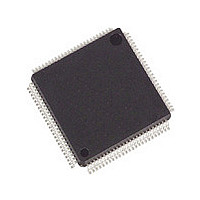
M30624FGPGP Renesas Electronics America, M30624FGPGP Datasheet - Page 99

M30624FGPGP
Manufacturer Part Number
M30624FGPGP
Description
Manufacturer
Renesas Electronics America
Datasheet
1.M30624FGPGP.pdf
(103 pages)
Specifications of M30624FGPGP
Cpu Family
M16C
Device Core Size
16/32Bit
Frequency (max)
24MHz
Interface Type
I2C/IEBus/UART
Program Memory Type
Flash
Program Memory Size
256KB
Total Internal Ram Size
20KB
# I/os (max)
87
Number Of Timers - General Purpose
11
Operating Supply Voltage (typ)
5V
Operating Supply Voltage (max)
5.5V
Operating Supply Voltage (min)
3.3V
On-chip Adc
26-chx10-bit
On-chip Dac
2-chx8-bit
Instruction Set Architecture
CISC
Mounting
Surface Mount
Pin Count
100
Package Type
LQFP
Lead Free Status / Rohs Status
Compliant
Available stocks
Company
Part Number
Manufacturer
Quantity
Price
Company:
Part Number:
M30624FGPGP
Manufacturer:
RENESAS
Quantity:
14
Part Number:
M30624FGPGP
Manufacturer:
RENESAS/瑞萨
Quantity:
20 000
Company:
Part Number:
M30624FGPGP#D3C
Manufacturer:
Renesas Electronics America
Quantity:
10 000
Company:
Part Number:
M30624FGPGP#D5C
Manufacturer:
Renesas Electronics America
Quantity:
10 000
Company:
Part Number:
M30624FGPGP#U3C
Manufacturer:
AVX
Quantity:
40 000
Company:
Part Number:
M30624FGPGP#U3C
Manufacturer:
Renesas
Quantity:
1 200
Company:
Part Number:
M30624FGPGP#U3C
Manufacturer:
Renesas Electronics America
Quantity:
10 000
Company:
Part Number:
M30624FGPGP#U5
Manufacturer:
RENESAS
Quantity:
1
Company:
Part Number:
M30624FGPGP#U5C
Manufacturer:
RENESAS
Quantity:
1 467
Rev.
1.10
2.00
REVISION HISTORY
May 28, 2003
Oct 29, 2003
Date
30-31
30-32
36-39
40-41
47-48
47-48
53-56
57-58
12-15
17,19
18,20
31-32
Page
4-5
2-4
2-4
7-9
22
23
24
30
31
32
42
47
48
49
11
30
1
2
6
-
Applications are partly revised.
Table 1.1.1 is partly revised.
Table 1.1.2 and 1.1.3 is partly revised.
“Note 1” is partly revised.
Table 1.5.3 is partly revised.
Table 1.5.5 is partly revised.
Table 1.5.6 is added.
Table 1.5.9 is partly revised.
Notes 1 and 2 in Table 1.5.26 is partly revised.
Notes 1 in Table 1.5.27 is partly revised.
Note 3 is added to “Data output hold time (refers to BCLK)” in Table 1.5.26
and 1.5.27.
Note 4 is added to “th(ALE-AD)” in Table 1.5.28.
Switching Characteristics is partly revised.
th(WR-AD) and th(WR-DB) in Figure 1.5.5 to 1.5.8 is partly revised.
th(ALE-AD), th(WR-CS), th(WR-DB) and th(WR-AD) in Figure 1.5.9 to
1.5.10 is partly revised.
Note 2 is added to Table 1.5.29.
Notes 1 and 2 in Table 1.5.45 is partly revised.
Notes 1 in Table 1.5.46 is partly revised.
Note 3 is added to “Data output hold time (refers to BCLK)” in Table
1.5.45 and 1.5.46.
Note 4 is added to “th(ALE-AD)” in Table 1.5.47.
Switching Characteristics is partly revised.
th(WR-AD) and th(WR-DB) in Figure 1.5.15 to 1.5.18 is partly revised.
th(ALE-AD), th(WR-CS), th(WR-DB) and th(WR-AD) in Figure 1.5.19 to
1.5.20 is partly revised.
Since high reliability version is added, a group name is revised.
M16C/62 Group (M16C/62P) → M16C/62 Group (M16C/62P, M16C/62PT)
Table 1.1 to 1.3 are revised.
Note 3 is partly revised.
Table 1.1 to 1.3 are revised.
Note 3 is partly revised.
Figure 1.2 Note5 is deleted.
Table 1.4 to 1.7 Product List is partly revised.
Table 1.8 and Figure 1.4 are added.
Figure 1.5 to 1.9 ZP is added.
Table 1.10 and 1.12 ZP is added to timer A.
Table 1.11 and 1.13 VCC1 is added to VREF.
Table 5.1 is revised.
Table 5.2 and 5.3 are revised.
M16C/62P Group (M16C/62P, M16C/62PT) Hardware Manual
C - 1
Description
Summary


