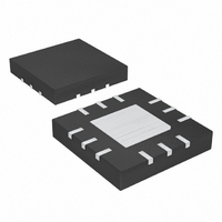
MAX4704ETC+T Maxim Integrated Products, MAX4704ETC+T Datasheet

MAX4704ETC+T
Specifications of MAX4704ETC+T
Related parts for MAX4704ETC+T
MAX4704ETC+T Summary of contents
Page 1
... INH 4 LOGIC GND 5 μMAX ________________________________________________________________ Maxim Integrated Products For pricing, delivery, and ordering information, please contact Maxim/Dallas Direct! at 1-888-629-4642, or visit Maxim’s website at www.maxim-ic.com. 4:1 Analog Multiplexer in QFN ♦ 3mm x 3mm 12-Pin QFN Package ♦ Guaranteed On-Resistance: 60Ω (max) (+2.7V Supply) 40Ω ...
Page 2
Low-Voltage, 60 Ω , 4:1 Analog Multiplexer in QFN ABSOLUTE MAXIMUM RATINGS (Voltages Referenced to GND) V+ .............................................................................-0.3V to +6V All Other Pins (Note 1)................................ -0.3V to (V+ + 0.3V) Continuous Current COM, NO_ ........................................±20mA Peak Current COM, NO_ (pulsed ...
Page 3
ELECTRICAL CHARACTERISTICS—Single +3V Supply (continued) (V+ = +2.7V to +3.3V +1.4V +25°C.) (Notes PARAMETER SYMBOL On-Channel -3dB Bandwidth BW Off-Isolation (Note 8) V ISO Crosstalk (Note NO_ ...
Page 4
Low-Voltage, 60 Ω , 4:1 Analog Multiplexer in QFN ELECTRICAL CHARACTERISTICS—Single +5V Supply (continued) (V+ = +4.5V to +5.5V +2.0V +25°C.) (Notes PARAMETER SYMBOL COM Off-Leakage Current ...
Page 5
A ON-RESISTANCE V VS. COM (V) ...
Page 6
Low-Voltage, 60 Ω , 4:1 Analog Multiplexer in QFN (T = +25°C, unless otherwise noted.) A INHIBIT TURN-ON/OFF TIME vs. TEMPERATURE ...
Page 7
PIN NAME µMAX QFN- — N. NO2 2 4 NO3 3 5 NO1 4 6 INH 5 7 GND 6 9 ADDB 7 10 ADDA 8 11 NO0 9 12 COM — — ...
Page 8
Low-Voltage, 60 Ω , 4:1 Analog Multiplexer in QFN ADD ADDA ADDB NO1–NO2 MAX4704 INH GND Figure 2. Address Transition Time V+ V+ ADDA ADDB NO1–NO3 MAX4704 V INH INH COM GND Figure 3. Inhibit Switching Times ...
Page 9
V+ V+ CHANNEL ADDB SELECT MAX4704 ADDA V INH INH GND REPEAT TEST FOR EACH SECTION. Figure 5. Charge Injection ADDA CHANNEL SELECT ADDB INH MEASUREMENTS ARE STANDARDIZED AGAINST SHORT AT SOCKET TERMINALS. OFF-ISOLATION IS MEASURED BETWEEN COM AND "OFF" ...
Page 10
Low-Voltage, 60 Ω , 4:1 Analog Multiplexer in QFN For the latest package outline information and land patterns www.maxim-ic.com/packages. PACKAGE TYPE 12 QFN-EP 10 µMAX 10 ______________________________________________________________________________________ Package Information PACKAGE CODE G1233-1 — DOCUMENT NO. 21-0102 21-0061 ...
Page 11
... Maxim cannot assume responsibility for use of any circuitry other than circuitry entirely embodied in a Maxim product. No circuit patent licenses are implied. Maxim reserves the right to change the circuitry and specifications without notice at any time. Maxim Integrated Products, 120 San Gabriel Drive, Sunnyvale, CA 94086 408-737-7600 ____________________ 11 © 2008 Maxim Integrated Products Low-Voltage, 60 Ω ...


