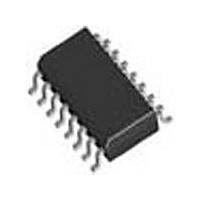
TC74HC123AFN Toshiba, TC74HC123AFN Datasheet - Page 3

TC74HC123AFN
Manufacturer Part Number
TC74HC123AFN
Description
Manufacturer
Toshiba
Datasheet
1.TC74HC123AFN.pdf
(14 pages)
Specifications of TC74HC123AFN
Logic Family
HC
High Level Output Current
-5.2mA
Low Level Output Current
5.2mA
Quiescent Current
4uA
Number Of Elements
2
Operating Temperature Classification
Industrial
Operating Supply Voltage (max)
6V
Operating Supply Voltage (typ)
2.5/3.3/5V
Operating Temperature (min)
-40C
Operating Temperature (max)
85C
Technology
CMOS
Abs. Propagation Delay Time
295ns
Operating Supply Voltage (min)
2V
Lead Free Status / Rohs Status
Not Compliant
Block Diagram (Note 1)(Note 2)
Truth Table
Note 1: Cx, Rx, Dx are external
Note 2: External clamping diode, Dx;
X: Don’t care
A
H
X
L
L
X
Inputs
H
H
capacitor, resistor, and diode, respectively.
The external capacitor is charged to V
If the supply voltage is turned off, Cx is discharges mainly through the internal (parasitic) diode. If Cx is
sufficiently large and V
current or latch-up. If the capacitance of the supply voltage filter is large enough and V
in rush current is automatically limited and damage to the IC is avoided.
The maximum value of forward current through the parasitic diode is ±20 mA.
In the case of a large Cx, the limit of fall time of the supply voltage is determined as follows:
In the event a system does not satisfy the above condition, an external clamping diode (Dx) is needed to
protect the IC from in rush current.
B
X
X
L
t
(tf is the time between the supply voltage turn off and the supply voltage reaching 0.4 V
f
CLR
≥ (V
H
H
H
H
L
CC
− 0.7) Cx/20 mA
Q
L
L
L
Outputs
Q
H
H
H
CC
drops rapidly, there will be some possibility of damaging the IC through in rush
Output Enable
Output Enable
Output Enable
Function
Inhibit
Inhibit
Inhibit
CC
level in the wait state, i.e. when no trigger is applied.
3
TC74HC123AP/AF/AFN
CC
drops slowly, the
CC
2007-10-01
.)


