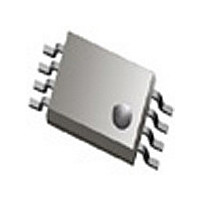
CAT24C02YI ON Semiconductor, CAT24C02YI Datasheet

CAT24C02YI
Specifications of CAT24C02YI
Available stocks
Related parts for CAT24C02YI
CAT24C02YI Summary of contents
Page 1
... I C CMOS Serial EEPROM Description The CAT24C01/02/04/08/16 are 1−Kb, 2−Kb, 4−Kb, 8−Kb and 16−Kb respectively CMOS Serial EEPROM devices organized internally as 8/16/32/64 and 128 pages respectively of 16 bytes each. All devices support both the Standard (100 kHz) as well as Fast 2 (400 kHz protocol. ...
Page 2
Table 1. ABSOLUTE MAXIMUM RATINGS Parameters Storage Temperature Voltage on any pin with respect to Ground (Note 1) Stresses exceeding Maximum Ratings may damage the device. Maximum Ratings are stress ratings only. Functional operation above the Recommended Operating Conditions is ...
Page 3
Table 4. PIN IMPEDANCE CHARACTERISTICS ( −40°C to +125°C and Symbol Parameter C (Note 4) SDA Pin Capacitance IN Other Pins I (Note 5) WP Input Current WP 4. ...
Page 4
... SCL: The Serial Clock input pin accepts the Serial Clock generated by the Master. SDA: The Serial Data I/O pin receives input data and transmits data stored in EEPROM. In transmit mode, this pin is open drain. Data is acquired on the positive edge, and is delivered on the negative edge of SCL. ...
Page 5
SCL SDA START CONDITION BUS RELEASE DELAY (TRANSMITTER) SCL FROM MASTER DATA OUTPUT FROM TRANSMITTER DATA OUTPUT FROM RECEIVER START SCL t SU:STA t HD:SDA ...
Page 6
Byte Write In Byte Write mode, the Master sends the START condition and the Slave address with the R/W bit set to zero to the Slave. After the Slave generates an acknowledge, the Master sends the byte address that is ...
Page 7
SCL th SDA 8 Bit Byte n S BUS ACTIVITY SLAVE R MASTER ADDRESS SLAVE ADDRESS BYTE 1 SCL a 7 SDA WP ACK t WR STOP ...
Page 8
Immediate Read Upon receiving a Slave address with the R/W bit set to ‘1’, the CAT24Cxx will interpret this as a request for data residing at the current byte address in memory. The CAT24Cxx will acknowledge the Slave address, will ...
Page 9
PIN # 1 IDENTIFICATION D TOP VIEW SIDE VIEW Notes: (1) All dimensions are in millimeters. (2) Complies with JEDEC MS-001. PACKAGE DIMENSIONS PDIP−8, 300 mils CASE 646AA−01 ISSUE A SYMBOL ...
Page 10
PIN # 1 IDENTIFICATION TOP VIEW SIDE VIEW Notes: (1) All dimensions are in millimeters. Angles in degrees. (2) Complies with JEDEC MS-012. PACKAGE DIMENSIONS SOIC 8, 150 mils CASE 751BD−01 ISSUE O SYMBOL ...
Page 11
E1 e TOP VIEW SIDE VIEW Notes: (1) All dimensions are in millimeters. Angles in degrees. (2) Complies with JEDEC MO-153. PACKAGE DIMENSIONS TSSOP8, 4.4x3 CASE 948AL−01 ISSUE O SYMBOL MIN A A1 0.05 A2 ...
Page 12
E E1 TOP VIEW SIDE VIEW Notes: (1) All dimensions are in millimeters. Angles in degrees. (2) Complies with JEDEC MO-187. PACKAGE DIMENSIONS MSOP 8, 3x3 CASE 846AD−01 ISSUE O SYMBOL MIN A A1 ...
Page 13
D E PIN#1 INDEX AREA TOP VIEW SYMBOL MIN NOM A 0.70 0.75 A1 0.00 0.02 A2 0.45 0.55 A3 0.20 REF b 0.20 0.25 D 1.90 2.00 D2 1.30 1.40 E 2.90 3.00 E2 1.20 1.30 e 0.50 TYP ...
Page 14
TOP VIEW SIDE VIEW Notes: (1) All dimensions are in millimeters. Angles in degrees. (2) Complies with JEDEC MO-193. PACKAGE DIMENSIONS TSOT−23, 5 LEAD CASE 419AE−01 ISSUE O SYMBOL MIN A A1 0.01 A2 ...
Page 15
... For the TDFN (VP2) package CAT24C02 new product, there is NO hyphen in the orderable part number (example: CAT24C02VP2IGT3A). 15. For additional package and temperature options, please contact your nearest ON Semiconductor Sales office. 16. For information on tape and reel specifications, including part orientation and tape sizes, please refer to our Tape and Reel Packaging Specifications Brochure, BRD8011/D ...
Page 16
... ON Semiconductor is licensed by Philips Corporation to carry the I ON Semiconductor and are registered trademarks of Semiconductor Components Industries, LLC (SCILLC). SCILLC reserves the right to make changes without further notice to any products herein. SCILLC makes no warranty, representation or guarantee regarding the suitability of its products for any particular purpose, nor does SCILLC assume any liability arising out of the application or use of any product or circuit, and specifically disclaims any and all liability, including without limitation special, consequential or incidental damages. “ ...


