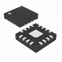
MAX4854HETE+ Maxim Integrated Products, MAX4854HETE+ Datasheet - Page 5

MAX4854HETE+
Manufacturer Part Number
MAX4854HETE+
Description
IC SWITCH DUAL SPDT 16TQFN
Manufacturer
Maxim Integrated Products
Datasheet
1.MAX4854HETET.pdf
(8 pages)
Specifications of MAX4854HETE+
Function
Switch
Circuit
2 x SPDT
On-state Resistance
9 Ohm
Voltage Supply Source
Single Supply
Voltage - Supply, Single/dual (±)
2 V ~ 5.5 V
Operating Temperature
-40°C ~ 85°C
Mounting Type
Surface Mount
Package / Case
16-TQFN Exposed Pad
Lead Free Status / RoHS Status
Lead free / RoHS Compliant
The MAX4854H/MAX4854HL quad SPST switches have
low on-resistance, operate from a +2V to +5.5V supply,
and are fully specified for nominal 3.0V applications.
These devices feature overvoltage protection by
putting the switch into high-impedance mode when the
switch input exceeds V
These switches have low 27.5pF on-channel capaci-
tance, which allows for 12Mbps switching of the data sig-
nals for USB 2.0 full speed/1.1 applications. The
MAX4854H/MAX4854HL are designed to switch D+ and
D- USB signals with a guaranteed skew of less than 1ns
(see Figure 2) as measured from 50% of the input signal
to 50% of the output signal.
The logic inputs (IN_) accept up to +5.5V even if the
supply voltages are below this level. For example, with a
+3.3V V
1, 5, 7, 10
1, 5, 7, 10
2, 11
PIN
12
13
14
15
16
—
3
4
6
8
9
CC
supply, IN_ can be driven low to GND and
NO1, NO2,
NC1, NC2,
NO3, NO4
NC3, NC4
NAME
COM2
COM3
COM4
COM1
GND
N.C.
V
IN2
IN3
IN4
IN1
Applications Information
EP
CC
Quad SPST, High-Bandwidth, Signal Line
_______________________________________________________________________________________
Detailed Description
CC
Normally Open Terminals for Analog Switch (MAX4854H)
Normally Closed Terminals for Analog Switch (MAX4854HL)
No Connection. Internally not connected.
Digital Control Input for Analog Switch 2. A logic-low (MAX4854H) or logic-high (MAX4854HL) on IN2
opens switch 2 and a logic-high (MAX4854H) or logic-low (MAX4854HL) on IN2 connects COM2 to NO2.
Common Terminal for Analog Switch 2
Ground
Common Terminal for Analog Switch 3
Digital Control Input for Analog Switch 3. A logic-low (MAX4854H) or logic-high (MAX4854HL) on IN3
opens switch 3 and a logic-high (MAX4854H) or logic-low (MAX4854HL) on IN3 connects COM3 to NO3.
Common Terminal for Analog Switch 4
Digital Control Input for Analog Switch 4. A logic-low (MAX4854H) or logic-high (MAX4854HL) on IN4
opens switch 4 and a logic-high (MAX4854H) or logic-low (MAX4854HL) on IN4 connects COM4 to NO4.
Supply Voltage. Bypass V
Digital Control Input for Analog Switch 1. A logic-low (MAX4854H) or logic-high (MAX4854HL) on IN1
opens switch 1 and a logic-high (MAX4854H) or logic-low (MAX4854HL) on IN1 connects COM1 to NO1.
Common Terminal for Analog Switch 1
Exposed Paddle. Connect to PC board ground plane.
.
Digital Control Inputs
CC
to GND with a 0.01µF capacitor as close to the pin as possible.
high to +5.5V, allowing for mixing of logic levels in a
system. Driving IN_ rail-to-rail minimizes power con-
sumption. For a +2V supply voltage, the logic thresholds
are 0.5V (low) and 1.4V (high); for a +5V supply voltage,
the logic thresholds are 0.8V (low) and 1.8V (high).
The on-resistance of these switches changes very little
for analog input signals across the entire supply volt-
age range (see the Typical Operating Characteristics).
The switches are bidirectional, so the NO_ and COM_
pins can be either inputs or outputs.
Caution: Do not exceed the absolute maximum ratings
because stresses beyond the listed ratings may cause
permanent damage to the device.
Proper power-supply sequencing is recommended for
all CMOS devices. Always apply V
analog signals, especially if the analog signal is not
current limited.
FUNCTION
Protection Switch
Power-Supply Sequencing
Analog Signal Levels
Pin Description
CC
before applying
5


