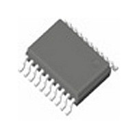
TC74LCX244FT Toshiba, TC74LCX244FT Datasheet - Page 3

TC74LCX244FT
Manufacturer Part Number
TC74LCX244FT
Description
Manufacturer
Toshiba
Datasheet
1.TC74LCX244FT.pdf
(11 pages)
Specifications of TC74LCX244FT
Logic Family
LCX
Logical Function
Buffer/Line Driver
Number Of Elements
2
Number Of Channels
8
Number Of Inputs
8
Number Of Outputs
8
Operating Supply Voltage (typ)
1.8/2.5/3.3V
Package Type
TSSOP
Output Type
3-State
Polarity
Non-Inverting
Propagation Delay Time
32ns
High Level Output Current
-24mA
Low Level Output Current
24mA
Operating Supply Voltage (max)
3.6V
Operating Supply Voltage (min)
1.65V
Quiescent Current
10uA
Technology
CMOS
Pin Count
20
Mounting
Surface Mount
Operating Temp Range
-40C to 85C
Operating Temperature Classification
Industrial
Lead Free Status / Rohs Status
Compliant
Available stocks
Company
Part Number
Manufacturer
Quantity
Price
Company:
Part Number:
TC74LCX244FT
Manufacturer:
Toshiba
Quantity:
90
Part Number:
TC74LCX244FT
Manufacturer:
TOSHIBA/东芝
Quantity:
20 000
Company:
Part Number:
TC74LCX244FT(EL)
Manufacturer:
TOSHIBA
Quantity:
6 603
Part Number:
TC74LCX244FT(EL)
Manufacturer:
TOSHIBA/东芝
Quantity:
20 000
Company:
Part Number:
TC74LCX244FT(ELM)
Manufacturer:
Toshiba
Quantity:
43 403
Absolute Maximum Ratings (Note 1)
Operating Ranges (Note 1)
Power supply voltage
DC input voltage
DC output voltage
Input diode current
Output diode current
DC output current
Power dissipation
DC V
Storage temperature
Note 1: Exceeding any of the absolute maximum ratings, even briefly, lead to deterioration in IC performance or
Note 2: Output in OFF state
Note 3: High or low state. I
Note 4: V
Power supply voltage
Input voltage
Output voltage
Output current
Operating temperature
Input rise and fall time
Note 1: The operating ranges must be maintained to ensure the normal operation of the device.
Note 2: Data retention only
Note 3: Output in OFF state
Note 4: High or low state
Note 5: V
Note 6: V
Note 7: V
CC
/ground current
even destruction.
Using continuously under heavy loads (e.g. the application of high temperature/current/voltage and the
significant change in temperature, etc.) may cause this product to decrease in the reliability significantly
even if the operating conditions (i.e. operating temperature/current/voltage, etc.) are within the absolute
maximum ratings and the operating ranges.
Please design the appropriate reliability upon reviewing the Toshiba Semiconductor Reliability Handbook
(“Handling Precautions”/“Derating Concept and Methods”) and individual reliability data (i.e. reliability test
report and estimated failure rate, etc).
Unused inputs must be tied to either V
Characteristics
Characteristics
OUT
CC
CC
IN
= 0.8 to 2.0 V, V
= 3.0 to 3.6 V
= 2.7 to 3.0 V
< GND, V
OUT
OUT
CC
> V
absolute maximum rating must be observed.
= 3.0 V
CC
I
CC
Symbol
Symbol
I
OH
V
V
dt/dv
I
V
V
T
T
OUT
V
I
V
P
OUT
OUT
I
OK
/I
CC
CC
opr
IK
stg
IN
IN
/I
D
GND
OL
CC
or GND.
− 0.5 to V
3
− 0.5 to 7.0
− 0.5 to 7.0
− 0.5 to 7.0 (Note 2)
− 65 to 150
1.65 to 3.6
1.5 to 3.6 (Note 2)
− 40 to 85
0 to V
0 to 5.5
0 to 5.5 (Note 3)
0 to 10 (Note 7)
Rating
Rating
± 100
− 50
± 50
± 50
180
± 24
± 12
CC
CC
+ 0.5
(Note 4)
(Note 4)
(Note 5)
(Note 6)
(Note 3)
ns/V
Unit
mW
Unit
mA
mA
mA
mA
mA
°C
°C
V
V
V
V
V
V
TC74LCX244F/FT/FK
2010-01-31


