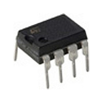
M24C01-BN6 STMicroelectronics, M24C01-BN6 Datasheet - Page 23

M24C01-BN6
Manufacturer Part Number
M24C01-BN6
Description
Manufacturer
STMicroelectronics
Datasheet
1.M24C01-BN6.pdf
(40 pages)
Specifications of M24C01-BN6
Density
1Kb
Interface Type
Serial (I2C)
Organization
128x8
Access Time (max)
900ns
Frequency (max)
400KHz
Write Protection
Yes
Data Retention
40Year
Operating Supply Voltage (typ)
5V
Package Type
PDIP
Operating Temp Range
-40C to 85C
Supply Current
2mA
Operating Supply Voltage (min)
4.5V
Operating Supply Voltage (max)
5.5V
Operating Temperature Classification
Industrial
Mounting
Through Hole
Pin Count
8
Lead Free Status / Rohs Status
Not Compliant
Available stocks
Company
Part Number
Manufacturer
Quantity
Price
M24C16, M24C08, M24C04, M24C02, M24C01
Table 12.
1. The device is not selected after a power-up, after a read command (after the Stop condition), or after the completion of the
Table 13.
Figure 11. AC measurement I/O waveform
Table 14.
1. Characterized only.
Symbol
I
Symbol
V
Symbol
internal write cycle t
V
I
I
CC1
V
I
CC
LO
Z
Z
LI
OL
IH
IL
C
C
t
WCH
WCL
C
NS
IN
IN
L
Input leakage current (SCL, SDA,
E0, E1,and E2)
Output leakage current
Supply current
Standby supply current
Input low voltage (SDA, SCL, WC)
Input high voltage (SDA, SCL, WC)
Output low voltage
DC characteristics (M24Cxx-F)
AC measurement conditions
Input parameters
Input capacitance (SDA)
Input capacitance (other pins)
WC input impedance
WC input impedance
Pulse width ignored (input filter on
SCL and SDA)
Load capacitance
Input rise and fall times
Input levels
Input and output timing reference levels
W
(t
Parameter
W
is triggered by the correct decoding of a write command).
Parameter
0.8V CC
0.2V CC
Input Levels
Parameter
(1)
Doc ID 5067 Rev 13
Device not selected
V
(in addition to those in
IN
V
OUT
= V
I
V
OL
Test condition
(rise/fall time < 50 ns)
SS
CC
V
= V
1.7 V
Single glitch
V
= 0.7 mA, V
Timing Reference Levels
IN
V
IN
Test condition
or V
= 1.7 V, f
CC
SS
> 0.7V
2.5 V
< 0.3 V
, V
CC
or V
mode
Input and Output
V
CC
, device in Standby
CC
CC
CC,
c
= 1.7 V
(1)
V
= 400 kHz
CC
CC
SDA in Hi-Z
, V
AI00825B
2.5 V
0.7V CC
0.3V CC
= 1.7 V
IN
Min.
Table
0.2V
0.3V
= V
SS
Min.
500
CC
CC
15
8)
or
100
to 0.8V
to 0.7V
0.7V
DC and AC parameters
–0.45
–0.45
Min.
Max.
CC
CC
50
CC
Max.
100
70
8
6
0.25 V
0.3 V
V
Max.
CC
± 2
± 2
0.8
0.2
1
+1
CC
CC
Unit
Unit
pF
ns
V
V
k
k
pF
pF
ns
Unit
23/40
mA
µA
µA
µA
V
V
V
V


