PI6C180VX Pericom Semiconductor, PI6C180VX Datasheet
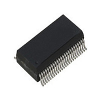
PI6C180VX

Manufacturer Part Number
PI6C180VX
Description
Manufacturer
Pericom Semiconductor
Datasheet

Specifications of PI6C180VX

Number Of Outputs
18
Operating Supply Voltage (max)
3.465V
Operating Temp Range
0C to 70C
Propagation Delay Time
8ns
Operating Supply Voltage (min)
3.135V
Mounting
Surface Mount
Pin Count
48
Operating Supply Voltage (typ)
3.3V
Package Type
SSOP
Duty Cycle
55%
Operating Temperature Classification
Commercial
Lead Free Status / Rohs Status
Not Compliant
Features
• High-speed, to 100 MHz
• Low-noise non-inverting 1-18 buffer
• Supports up to four SDRAM DIMMs
• Low skew (< 250ps) between any two output clocks
• I
• Multiple V
• 3.3V power supply voltage
• Separate Hi-Z pin for testing
• Packaging:
Block Diagram
- 48-pin SSOP (V)
2
C Serial Configuration interface
BUF_IN
DD
SCLOCK
, V
SDATA
SS
OE
pins for noise reduction
I 2 C
I/O
SDRAM0
SDRAM1
SDRAM2
SDRAM3
SDRAM17
1
Description
The PI6C180, a high-speed low-noise 1-18 non-inverting buffer
designed for SDRAM clock buffer applications operates up to
100 MHz.
At power up all SDRAM output are enabled and active. The I
Serial control may be used to individually activate/deactivate any
of the 18 output drivers.
The output enable (OE) pin may be pulled low to put all outputs
in a Hi-Z state.
Note:
Purchase of I
use them in an I
Pin Configuration
SDRAM16
SDRAM2
SDRAM3
SDRAM6
SDRAM7
SDRAM0
SDRAM1
SDRAM4
SDRAM5
2
BUF_IN
C components from Pericom conveys a license to
SDATA
V
2
V
V
V
V
V
V
V
V
C system as defined by Philips.
V
V
DDIIC
DD1
DD3
DD4
DD0
DD2
SS0
SS1
SS3
NC
NC
SS2
SS4
Precision 1-18 Clock Buffer
1
2
3
4
5
6
7
8
9
10
11
12
13
14
15
16
17
18
19
20
21
22
23
24
48
47
46
45
44
43
42
41
40
39
38
37
36
35
34
33
32
31
30
29
28
27
26
25
NC
NC
V
SDRAM15
SDRAM14
V
V
SDRAM13
SDRAM12
V
OE
V
SDRAM11
SDRAM10
V
V
SDRAM9
SDRAM8
V
V
SDRAM17
V
V
SCLOCK
DD9
SS9
DD8
SS8
DD7
SS7
DD6
SS6
DD5
SS5
SSIIC
PS8141F
PI6C180
12/13/04
2
C

Related parts for PI6C180VX

PI6C180VX Summary of contents

Page 1

Features • High-speed, to 100 MHz • Low-noise non-inverting 1-18 buffer • Supports up to four SDRAM DIMMs • Low skew (< 250ps) between any two output clocks 2 • Serial Configuration interface • Multiple ...

Page 2

Pin Description Pin Symbol SDRAM[0-3] 13, 14, 17, 18 SDRAM[4-7] 31, 32, 35, 36 SDRAM[8-11] 40, 41, 44, 45 SDRAM[12-15] 21, 28 SDRAM[16-17] 11 Buf_IN DATA 25 S CLOCK 3, 7, 12, ...

Page 3

I C Control 2 The I C interface permits individual enable/disable of each clock output and test mode enable. The PI6C180 is a slave receiver device. It can not be read back. Sub addressing is not supported. All ...

Page 4

DC Operating Specifications Symbol Parameter Input Voltage V Input High voltage IH V Input Low voltage IL I Input leakage current IL V [0-9] = 3.3V ± Output High voltage OH V Output Low voltage OL C Output ...

Page 5

Clocking Interface (TTL) Input Waveform Output Waveform Minimum & Maximum Expected Capacitive Loads Min. Max. Clock Units Load Load SDRAM Notes: 1. Maximum rise/fall times are guaranteed at maximum specified load. 2. Minimum rise/fall times are ...

Page 6

PCB Layout Suggestion C1 VDD VSS C2 VDD VSS C3 VDD VSS C4 VDD VSS C5 VDD VSS C6 VDD Notes: 1. This is only a suggested layout. There may be alternate solutions depending on actual PCB design and layout. ...

Page 7

... X.XX DENOTES DIMENSIONS X.XX IN MILLIMETERS Ordering Information Ordering Code PI6C180V PI6C180VE Notes: 1. Thermal characteristics can be found on the company web site at www.pericom.com/packaging/ Pericom Semiconductor Corporation • 1-800-435-2336 • www.pericom.com .395 .420 10.03 .291 10.67 .299 7.39 7.59 Gauge Plane .620 .630 15.75 ...

Related keywords