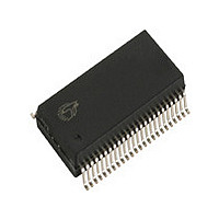
CY7C63413-PVXC Cypress Semiconductor Corp, CY7C63413-PVXC Datasheet - Page 22

CY7C63413-PVXC
Manufacturer Part Number
CY7C63413-PVXC
Description
Manufacturer
Cypress Semiconductor Corp
Datasheet
1.CY7C63413-PVXC.pdf
(32 pages)
Specifications of CY7C63413-PVXC
Cpu Family
enCoRe II
Device Core
M8C
Device Core Size
8b
Frequency (max)
12MHz
Interface Type
USB
Program Memory Type
EPROM
Program Memory Size
8KB
Total Internal Ram Size
256Byte
# I/os (max)
24
Number Of Timers - General Purpose
1
Operating Supply Voltage (typ)
5V
Operating Supply Voltage (max)
5.25/5.5V
Operating Supply Voltage (min)
4/4.35V
Instruction Set Architecture
RISC
Operating Temp Range
0C to 70C
Operating Temperature Classification
Commercial
Mounting
Surface Mount
Pin Count
48
Package Type
SSOP
Lead Free Status / Rohs Status
Compliant
Document #: 38-08027 Rev. *B
Figure 7. Decode table forTable 29: “Details of Modes for Differing Traffic Conditions”
The response of the SIE can be summarized as follows:
The In and Out PID status is updated at the end of a trans-
action.
1. the SIE will only respond to valid transactions, and will ig-
2. the SIE will generate IRQ when a valid transaction is
3. an incoming Data packet is valid if the count is <= 10 (CRC
4. a Setup will be ignored by all non-Control endpoints (in
5. an In will be ignored by an Out configured endpoint and vice
Encoding
End Point
Mode
3
Legend:
nore non-valid ones;
completed or when the DMA buffer is corrupted
inclusive) and passes all error checking;
appropriate modes);
versa.
2
1
0
Token
Setup
In
Out
Properties of incoming packet
count
The number of received bytes
UC: unchanged
x: don’t care
available for Control endpoint only
buffer
The quality status of the DMA buffer
The validity of the received data
dval
DTOG
TX: transmit
RX: receive
Status bits
DVAL
COUNT
The Setup PID status is updated at the beginning of the Data
packet phase.
The entire EndPoint 0 mode and the Count register are locked
to CPU writes at the end of any transaction in which an ACK
is transferred. These registers are only unlocked upon a CPU
read of these registers, and only if that read happens after the
transaction completes. This represents about a 1-µs window
to which to the CPU is locked from register writes to these USB
registers. Normally the firmware does a register read at the
beginning of the ISR to unlock and get the mode register infor-
mation. The interlock on the Mode and Count registers
ensures that the firmware recognizes the changes that the SIE
might have made during the previous transaction.
TX0: transmit 0-length packet
Set-
up
PID Status bits
In
What the SIE does to Mode bits
Out
Acknowledge phase completed
ACK
End Point
Mode
3
CY7C63413C
CY7C63513C
CY7C63613C
2 1 0
Page 22 of 32
Interrupt?
Re-
sponse
In
t
[+] Feedback


