CY7C1011CV33-12BVI Cypress Semiconductor Corp, CY7C1011CV33-12BVI Datasheet
CY7C1011CV33-12BVI
Specifications of CY7C1011CV33-12BVI
Available stocks


Related parts for CY7C1011CV33-12BVI


CY7C1011CV33-12BVI Summary of contents
Page 1
... Cypress Semiconductor Corporation Document Number: 38-05232 Rev. *I 2-Mbit (128K x 16) Static RAM Functional Description The CY7C1011CV33 is a high performance CMOS static RAM organized as 131,072 words by 16 bits. This device has an automatic power down feature that significantly reduces power consumption when deselected. ...
Page 2
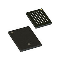
... NC pins are not connected on the die. Document Number: 38-05232 Rev. *I [1] Figure 2. 48-Ball VFBGA Pinout BLE OE BHE I/O BLE I/O 15 I/O I/O 14 I I/O 11 I/O 10 I Figure 3. 44-Pin TQFP CY7C1011CV33 [ BHE CE I I/O I/O I I I I/O I/O I ...
Page 3
... Selection Guide Description Maximum Access Time Maximum Operating Current Maximum CMOS Standby Current Document Number: 38-05232 Rev. *I -10 10 Industrial 100 Automotive-A 100 Automotive-E Industrial 10 Automotive-A 10 Automotive-E CY7C1011CV33 -12 Unit 120 Page [+] Feedback ...
Page 4
... MAX Automotive-A Automotive -E Max > V – 0.3V, Industrial > V – 0.3V Automotive-A V < 0.3V Automotive -E CY7C1011CV33 Ambient V CC Temperature ( 3.3V 10% –40C to +85C –40C to +85C –40C to +125C -10 -12 Unit Min Max Min Max 2.4 2 ...
Page 5
... Still Air, soldered × 4.5 inch, four-layer printed circuit board Figure 4. AC Test Loads and Waveforms 12-ns devices: 50 30 pF* 1.5V (a) High-Z characteristics: 90% 10% (c) Fall Time: 1 V/ns Figure 4 Figure 4 (d). CY7C1011CV33 . Max Unit TSOP II TQFP VFBGA 44.56 42.66 46.98 10.75 14.64 9 ...
Page 6
... The minimum write cycle time for Write Cycle No. 3 (WE controlled, OE LOW) is the sum of t Document Number: 38-05232 Rev. *I Description Industrial/Automotive-A Automotive-E Industrial/Automotive-A Automotive-E values until the first memory access is performed less than less than t , and t LZCE HZOE LZOE HZWE “AC Test Loads and Waveforms and t HZWE CY7C1011CV33 -10 -12 Min Max Min Max ...
Page 7
... Device is continuously selected. OE, CE, BHE, and/or BLE = V 11 HIGH for read cycle. 12. Address valid prior to or coincident with CE transition LOW. Document Number: 38-05232 Rev OHA DOE t LZOE DBE DATA VALID 50 CY7C1011CV33 [10, 11] DATA VALID [11, 12] t HZOE t HZCE t HZBE HIGH IMPEDANCE 50 Page [+] Feedback ...
Page 8
... SA BHE, BLE WE CE DATA I/O Notes 13. Data I/O is high impedance if OE, BHE, and/or BLE = V 14 goes HIGH simultaneously with WE going HIGH, the output remains in a high impedance state. Document Number: 38-05232 Rev. *I [13, 14 SCE PWE PWE t SCE CY7C1011CV33 Page [+] Feedback ...
Page 9
... Read – Lower Bits Only High Z Data Out Read – Upper Bits Only Data In Data In Write – All Bits Data In High Z Write – Lower Bits Only High Z Data In Write – Upper Bits Only High Z High Z Selected, Outputs Disabled CY7C1011CV33 LZWE Power Standby ( Active ( Active (I ) ...
Page 10
... CY7C1011CV33-10ZSXA 51-85087 44-pin TSOP II (Pb-Free) 12 CY7C1011CV33-12AXI 51-85064 44-pin TQFP (Pb-Free) CY7C1011CV33-12ZSXE 51-85087 44-pin TSOP II (Pb-Free) Package Diagrams Figure 10. 44-Pin Thin Small Outline Package Type II, 51-85087 Document Number: 38-05232 Rev. *I CY7C1011CV33 Package Type Industrial Automotive-A Industrial Automotive-E 51-85087 *C Operating Range Page [+] Feedback ...
Page 11
... Package Diagrams (continued) Figure 11. 44-Pin Thin Plastic Quad Flat Pack, 51-85064 Document Number: 38-05232 Rev. *I CY7C1011CV33 51-85064 *D Page [+] Feedback ...
Page 12
... Package Diagrams (continued) Figure 12. 48-Ball VFBGA ( mm), 51-85150 Document Number: 38-05232 Rev. *I CY7C1011CV33 51-85150 *E Page [+] Feedback ...
Page 13
... Document History Page Document Title: CY7C1011CV33, 2-Mbit (128K x 16) Static RAM Document Number: 38-05232 Orig. of REV. ECN NO. Issue Date Change ** 117132 07/31/02 HGK *A 118057 08/19/02 HGK *B 119702 10/11/02 DFP *C 386106 See ECN PCI *D 498501 See ECN NXR *E 522620 See ECN VKN ...