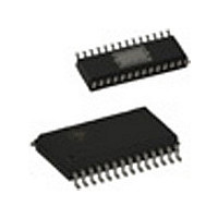
CY6264-70SNI Cypress Semiconductor Corp, CY6264-70SNI Datasheet

CY6264-70SNI
Specifications of CY6264-70SNI
Available stocks
Related parts for CY6264-70SNI
CY6264-70SNI Summary of contents
Page 1
... Cypress Semiconductor Corporation Document #: 001-02367 Rev. ** power-down feature (CE by over 70% when deselected. The CY6264 is packaged in a 450-mil (300-mil body) SOIC. An active LOW write enable signal (WE) controls the writing/reading operation of the memory. When CE , and OE 2 inputs are both LOW and CE input/output pins (I/O ...
Page 2
... Max., = GND = Max., Com’ Ind’ > V Com’ IH, Ind’ > V – 0.3V, Com’ > V – 0. < 0. Ind’l CY6264 CY6264-70 Unit 70 ns 100 mA 200 20/ Ambient Temperature V CC ° ° 5V ± 10 +70 C ° ° – +85 C 6264-55 6264-70 Max ...
Page 3
... Tested initially and after any design or process changes that may affect these parameters. Document #: 001-02367 Rev. ** [3] 6264-55 Min Test Conditions T = 25° MHz 5. less than t for any given device. HZCE LZCE LOW, CE HIGH, and WE LOW. Both signals must be LOW to initiate a write and either 1 2 CY6264 6264-70 Max. Min. Max. Unit ...
Page 4
... WE is HIGH for read cycle. 11. Data I/O is High Document #: 001-02367 Rev 481Ω 3. GND 255Ω JIG AND SCOPE (b) 1.73V OHA DOE DATA VALID 50 IH CY6264 ALL INPUT PULSES 90% 90% 10% 10% < < DATA VALID t HZOE t HZCE HIGH IMPEDANCE t PD 50% Page ICC ISB [+] Feedback ...
Page 5
... DATA UNDEFINED Note: 12 goes HIGH simultaneously with WE HIGH, the output remains in a high-impedance state. Document #: 001-02367 Rev SCE1 t SCE2 PWE t SD DATA VALID IN t HZWE HIGH IMPEDANCE SCE1 SCE2 PWE t SD DATA VALID IN t HZWE CY6264 LZWE HIGH IMPEDANCE Page [+] Feedback ...
Page 6
... TYPICAL ACCESS TIME CHANGE vs. OUTPUT LOADING 30.0 25.0 20.0 15.0 10.0 V =4. =25°C A 5.0 0.0 0 200 400 600 800 1000 CAPACITANCE (pF) CY6264 OUTPUT SOURCE CURRENT vs. OUTPUT VOLTAGE 120 100 80 V =5. =25° 0.0 1.0 2.0 3.0 4.0 OUTPUT VOLTAGE (V) OUTPUT SINK CURRENT vs ...
Page 7
... Truth Table Address Designators Address Name A10 A11 A12 Document #: 001-02367 Rev Input/Output X High Z Deselect/Power-Down X High Z Deselect L Data Out Read X Data In Write H High Z Deselect Address Function CY6264 Mode Pin Number Page [+] Feedback ...
Page 8
... Ordering Code 55 CY6264-55SC 70 CY6264-70SC 55 CY6264-55SNC 55 CY6264-55SNXC 70 CY6264-70SNC 70 CY6264-70SNXC 70 CY6264-70SNI 70 CY6264-70SNXI Shaded areas contain advance information. Package Diagrams 28-lead (300 mil) SNC Package Outline (Narrow Body) SN28 0.702 0.710 Note: 13. Not recommended for new designs. A 0.050 TYP. Document #: 001-02367 Rev. ** Package ...
Page 9
... SOIC with Wide Body S28.33 PIN 1 ID DIMENSIONS IN INCHES[MM] PACKAGE WEIGHT 0.79gms 0.460[11.684] 0.480[12.192] 0.338[8.585] 0.346[8.788] SEATING PLANE 0.094[2.387] 0.110[2.794] 0.004[0.102] 0.002[0.050] 0.014[0.355] CY6264 MIN. MAX. PART # S28.33 STANDARD PKG. SZ28.33 LEAD FREE PKG. 0.008[0.203] 0.030[0.762] 0.012[0.304] 0.050[1.270] 51-85058-*B Page [+] Feedback ...
Page 10
... Document History Page Document Title:CY6264 Static RAM Document Number: 001-02367 Orig. of REV. ECN NO. Issue Date Change ** 384870 See ECN Document #: 001-02367 Rev. ** Description of Change PCI Spec # change from 38-00425 to 001-02367 CY6264 Page [+] Feedback ...


