CY62168DV30LL-70BVI Cypress Semiconductor Corp, CY62168DV30LL-70BVI Datasheet
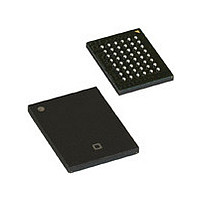
CY62168DV30LL-70BVI

Manufacturer Part Number
CY62168DV30LL-70BVI
Description
Manufacturer
Cypress Semiconductor Corp
Datasheet

Specifications of CY62168DV30LL-70BVI

Density
16Mb
Access Time (max)
70ns
Sync/async
Asynchronous
Architecture
Not Required
Clock Freq (max)
Not RequiredMHz
Operating Supply Voltage (typ)
3V
Address Bus
21b
Package Type
VFBGA
Operating Temp Range
-40C to 85C
Number Of Ports
1
Supply Current
25mA
Operating Supply Voltage (min)
2.2V
Operating Supply Voltage (max)
3.6V
Operating Temperature Classification
Industrial
Mounting
Surface Mount
Pin Count
48
Word Size
8b
Number Of Words
2M
Lead Free Status / Rohs Status
Not Compliant

Available stocks

Company
Part Number
Manufacturer
Quantity
Price
Part Number:
CY62168DV30LL-70BVI
Manufacturer:
CY
Quantity:
764
Cypress Semiconductor Corporation
Document #:
Features
Functional Description
The CY62168DV30 is a high-performance CMOS static RAM
organized as 2048K words by eight bits. This device
advanced circuit design to provide ultra-low active current.
This is ideal for providing More Battery Life
portable applications such as cellular telephones.
also has an automatic power-down feature that significantly
reduces power consumption by
toggling. The device can be put into standby mode reducing
Note:
1.
• Very
• Wide
• Ultra-low active power
• Ultra-low standby power
• Easy memory expansion with
• Automatic power-down when deselected
• CMOS for optimum speed/power
• Packages offered in a 48-ball FBGA
features
— Typical active current:
Logic Block Diagram
For best practice recommendations, please refer to the Cypress application note “System Design Guidelines” on http://www.cypress.com.
high speed:
voltage range: 2.2V to 3.6V
38-05329
CE
CE
1
2
55 ns and 70 ns
Rev.
*B
[1]
2
15
90%
mA @ f = 1 MHz
mA @ f = f
CE
when addresses are not
WE
OE
1
, CE
A
A
A
A
A
A
A
A
A
A
A
A
A
11
12
10
9
0
1
2
3
4
5
6
7
8
2
MAX
, and OE
3901 North First Street
(MoBL
The device
PRELIMINARY
features
®
) in
8192 x 256 x 8
Data in Drivers
RAM ARRAY
2048K x 8
DECODER
COLUMN
power consumption by more than 99% when deselected
Enable 1 (CE
input/output pins
high-impedance state when: deselected
HIGH or Chip Enable 2 (CE
HIGH), or during a write operation
and Chip Enable 2 (CE
Writing to the device is accomplished by taking Chip Enable 1
(CE
(WE) input LOW. Data on the eight I/O pins (I/O
is then written into the location specified on the address pins
(A
Reading from the device is accomplished by taking Chip
Enable 1 (CE
Output Enable (OE) LOW while forcing the Write Enable (WE)
HIGH. Under these conditions, the contents of the memory
location specified by the address pins will appear on the I/O
pins. The eight input/output pins (I/O
in a high-impedance state when the device is
LOW and CE
during a write operation (CE
LOW). See the truth table at the back of this data sheet for a
complete description of read and write modes.
0
1
through A
16M (2048K
) LOW and Chip Enable 2 (CE
POWER
DOWN
2
20
1
1
HIGH), the outputs are disabled (OE HIGH), or
) HIGH or Chip Enable 2 (CE
) LOW and Chip Enable 2 (CE
San Jose
).
(I/O
2
0
) HIGH and WE LOW).
,
through I/O
CA 95134
2
) LOW, outputs are disabled (OE
1
x 8) Static RAM
LOW and CE
(Chip Enable 1 (CE
2
CY62168DV30
0
) HIGH and Write Enable
through I/O
I/O
I/O
I/O
I/O
I/O
I/O
I/O
I/O
Revised April 24, 2003
7
) are placed in a
Chip Enable 1 (CE
0
1
2
3
4
5
6
7
2
deselected(CE
2
HIGH and WE
0
) LOW . The
408-943-2600
2
through I/O
7
) HIGH and
MoBL
) are placed
1
) LOW
Chip
1
7
1
®
)
)

Related parts for CY62168DV30LL-70BVI

CY62168DV30LL-70BVI Summary of contents

Page 1

... The device can be put into standby mode reducing Logic Block Diagram Note: 1. For best practice recommendations, please refer to the Cypress application note “System Design Guidelines” on http://www.cypress.com. Cypress Semiconductor Corporation Document #: 38-05329 Rev. *B PRELIMINARY 16M (2048K power consumption by more than 99% when deselected Enable 1 (CE ...

Page 2

Pin Configuration Note: 2. DNU pins are to be connected left open. SS Document #: 38-05329 Rev. *B PRELIMINARY FBGA Top View DNU ...

Page 3

... Supply Voltage to Ground Potential . DC Voltage Applied to Outputs [3] in High-Z State .................................... Product Portfolio V Range(V) CC Product Min. Typ. CY62168DV30L 2.2 3.0 CY62168DV30LL 2.2 3.0 DC Electrical Characteristics Parameter Description V Output HIGH Voltage OH V Output LOW Voltage OL V Input HIGH Voltage IH V Input LOW Voltage ...

Page 4

Capacitance Parameter C Input Capacitance IN C Output Capacitance OUT Thermal Resistance Parameter Description Thermal Resistance (Junction to Ambient) JA Thermal Resistance (Junction to Case Test Loads and Waveforms OUTPUT ...

Page 5

Data Retention Waveform Switching Characteristics (Over the Operating Range) Parameter Description Read Cycle t Read Cycle Time RC t Address to Data Valid AA t Data Hold from Address Change OHA t ...

Page 6

Switching Waveforms Read Cycle No. 1 (Address Transition Controlled) ADDRESS DATA OUT PREVIOUS DATA VALID [13, 14] Read Cycle No. 2 (OE Controlled) ADDRESS HIGH IMPEDANCE DATA OUT t LZCE ...

Page 7

Switching Waveforms (continued) Write Cycle No Controlled ADDRESS DATA I/O Write Cycle No. 3 (WE Controlled, OE LOW) ADDRESS DON’T CARE ...

Page 8

... Ordering Code 55 CY62168DV30L-55**I CY62168DV30LL-55**I 70 CY62168DV30L-70**I CY62168DV30LL-70**I Package Diagram MoBL is a registered trademark, and MoBL2 and More Battery Life are trademarks of Cypress Semiconductor. All product and company names mentioned in this document are the trademarks of their respective holders. Document #: 38-05329 Rev. ...

Page 9

Document History Page Document Title: CY62168DV30 MoBL Document Number: 38-05329 Issue REV. ECN NO. Date ** 118409 09/30/02 *A 123693 02/05/03 *B 126556 04/24/03 Document #: 38-05329 Rev. *B PRELIMINARY ® 16M (2048K x 8) Static RAM Orig. of Change ...

Related keywords