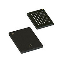
CY62157DV18LL-55BVI Cypress Semiconductor Corp, CY62157DV18LL-55BVI Datasheet - Page 3

CY62157DV18LL-55BVI
Manufacturer Part Number
CY62157DV18LL-55BVI
Description
Manufacturer
Cypress Semiconductor Corp
Datasheet
1.CY62157DV18LL-55BVI.pdf
(10 pages)
Specifications of CY62157DV18LL-55BVI
Density
8Mb
Access Time (max)
55ns
Sync/async
Asynchronous
Architecture
Not Required
Clock Freq (max)
Not RequiredMHz
Operating Supply Voltage (typ)
1.8V
Address Bus
19b
Package Type
VFBGA
Operating Temp Range
-40C to 85C
Number Of Ports
1
Supply Current
20mA
Operating Supply Voltage (min)
1.65V
Operating Supply Voltage (max)
1.95V
Operating Temperature Classification
Industrial
Mounting
Surface Mount
Pin Count
48
Word Size
16b
Number Of Words
512K
Lead Free Status / Rohs Status
Not Compliant
Available stocks
Company
Part Number
Manufacturer
Quantity
Price
Company:
Part Number:
CY62157DV18LL-55BVI
Manufacturer:
CY
Quantity:
80
Company:
Part Number:
CY62157DV18LL-55BVI
Manufacturer:
CYPRESS
Quantity:
173
Maximum Ratings
(Above which the useful life may be impaired. For user guide-
lines, not tested.)
Storage Temperature ................................. –65°C to +150°C
Ambient Temperature with
Power Applied............................................. –55°C to +125°C
Supply Voltage
to Ground Potential ......................... –0.2V to V
DC Voltage Applied to Outputs
in High-Z State
Product Portfolio
DC Electrical Characteristics
Capacitance
Document #: 38-05126 Rev. *B
CY62157DV18L
CY62157DV18LL
V
V
V
V
I
I
I
I
I
Notes:
IX
OZ
CC
SB1
SB2
4.
5.
6.
Parameter
OH
OL
IH
IL
V
Typical values are included for reference only and are not guaranteed or tested. Typical values are measured at V
Tested initially and after any design or process changes that may affect these parameters.
Product
IL
(min.) = –2.0V for pulse durations less than 20 ns.
Parameter
C
C
OUT
[4]
Output HIGH Voltage
Output LOW Voltage
Input HIGH Voltage
Input LOW Voltage
Input Leakage Current GND < V
Output Leakage
Current
V
Current
Automatic CE
Power-down Current –
CMOS Inputs
Automatic CE
Power-down Current –
CMOS Inputs
IN
[6]
CC
....................................–0.2V to V
Operating Supply
Description
Min.
1.65
1.65
V
CC
Typ.
Range(V)
1.8
1.8
[5]
Output Capacitance
Input Capacitance
(Over the Operating Range)
I
I
GND < V
Disabled
f = f
f = 1 MHz
CE
0.2V, V
< 0.2V, f = f
and Data Only), f = 0 (OE,
WE, BHE and BLE)
CE
0.2V, V
V
1.95V
OH
OL
IN
Description
1
1
= 0.1 mA
MAX
= 0.1 mA
< 0.2V, f = 0, V
> V
> V
Max.
1.95
1.95
IN
IN
CCMAX
Test Conditions
CC
CC
= 1/t
I
O
> V
> V
< V
< V
CC
MAX
CC
RC
CC
0.2V, CE
0.2V, CE
CC
+ 0.2V
+ 0.2V
CC
Speed
(Address
(ns)
55
70
55
70
, Output
0.2V, V
0.2V or
V
V
Vcc = 1.95V,
I
CMOS level
CC
OUT
CC
CC
2
2
=
= 1.65V
= 1.65V
= 0 mA,
<
<
IN
T
V
Typ.
A
CC
DC Input Voltage
Output Current into Outputs (LOW)............................. 20 mA
Static Discharge Voltage.......................................... > 2001V
(per MIL-STD-883, Method 3015)
Latch-up Current .................................................... > 200 mA
Operating Range
L
LL
L
LL
= 25°C, f = 1 MHz
Industrial
1
1
Range
f = 1 MHz
= V
[5]
Test Conditions
CC(typ)
Min.
–0.2
1.4
1.4
Operating, Icc (mA)
–1
–1
CY62157DV18-55
Max.
5
5
Ambient Temperature (T
Typ.
10
1
2
2
2
2
[4]
[5]
Power Dissipation
................................ –0.2V to V
–40 C to +85 C
Typ.
10
10
8
8
V
Max.
0.2
CC
0.2
0.4
+1
+1
20
20
20
f = f
[5]
5
5
5
CC
+
MAX
= V
Min.
–0.2
Max.
1.4
1.4
–1
–1
CC(typ)
20
15
20
15
CY62157DV18-70
Max.
6
8
, T
Typ.
A
A
CY62157DV18
)
Standby, I
8
1
2
2
2
2
= 25°C.
Typ.
[5]
2
2
2
2
1.65V to 1.95V
[5]
V
Max.
MoBL2
Page 3 of 10
0.2
0.2
0.4
CC
+1
+1
15
20
20
5
5
5
V
CC
Unit
SB2
pF
pF
CC
+
Max.
+ 0.2V
20
20
5
5
( A)
Unit
mA
V
V
V
V
A
A
A
A
[+] Feedback


