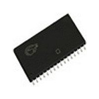
CY62148CV30LL-70BAI Cypress Semiconductor Corp, CY62148CV30LL-70BAI Datasheet

CY62148CV30LL-70BAI
Specifications of CY62148CV30LL-70BAI
Available stocks
Related parts for CY62148CV30LL-70BAI
CY62148CV30LL-70BAI Summary of contents
Page 1
... Cypress Semiconductor Corporation Document #: 38-05035 Rev. *A 512K x 8 MoBL Static RAM advanced circuit design to provide ultra-low active current. This is ideal for providing More Battery Life™ (MoBL™) in por- table applications such as cellular telephones. The device also has an automatic power-down feature that significantly reduc- es power consumption by 80% when addresses are not tog- gling ...
Page 2
Pin Configurations Maximum Ratings (Above which the useful life may be impaired. For user guide- lines, not tested.) Storage Temperature .... .............................–65°C to +150°C Ambient Temperature with Power Applied. ............................................–55°C to +125°C Supply Voltage to Ground Potential.....–0. ...
Page 3
Electrical Characteristics Over the Operating Range Parameter Description V Output HIGH Voltage Output LOW Voltage Input HIGH Voltage IH V Input LOW Voltage IL I Input Load Current GND < ...
Page 4
Parameter Description V Output HIGH Voltage Output LOW Voltage Input HIGH Voltage IH V Input LOW Voltage IL I Input Load Current GND < Output Leakage GND < V ...
Page 5
AC Test Loads and Waveforms OUTPUT INCLUDING JIG AND SCOPE Equivalent to: THÉ VENIN EQUIVALENT R TH OUTPUT Parameters 2.5V R1 16.6 R2 15 1.20 TH Data Retention Characteristics Parameter ...
Page 6
Switching Characteristics Over the Operating Range Parameter READ CYCLE t Read Cycle Time RC t Address to Data Valid AA t Data Hold from Address Change OHA t CE LOW to Data Valid ACE t OE LOW to Data Valid ...
Page 7
Switching Waveforms [12, 13] Read Cycle No. 1 ADDRESS DATA OUT PREVIOUS DATA VALID [13, 14] Read Cycle No ACE OE t LZOE HIGH IMPEDANCE DATA OUT t LZCE SUPPLY CURRENT [10, 15, ...
Page 8
Switching Waveforms (continued) [10, 15, 16] Write Cycle No. 2 (CE Controlled) ADDRESS DATA I/O Write Cycle No. 3 (WE Controlled, OE LOW) ADDRESS DATA I/O NOTE 17 t HZWE Document #: 38-05035 ...
Page 9
Typical DC and AC Parameters (Typical values are included for reference only and are not guaranteed or tested. Typical values are measured at V Operating Current vs. Supply Voltage 14.0 MoBL 12.0 10 55ns) 8.0 max ...
Page 10
... Ordering Information Speed (ns) Ordering Code 70 CY62148CV25LL-70BAI CY62148CV25LL-70BVI CY62148CV30LL-70BAI CY62148CV30LL-70BVI CY62148CV33LL-70BAI CY62148CV33LL-70BVI 55 CY62148CV25LL-55BAI CY62148CV25LL-55BVI CY62148CV30LL-55BAI CY62148CV30LL-55BVI CY62148CV33LL-55BAI CY62148CV33LL-55BVI Document #: 38-05035 Rev. *A Package Name Package Type BA36B 36-Ball Fine Pitch BGA ( 8 1.2 mm) BV36A 36-Ball Fine Pitch BGA ( mm) BA36B 36-Ball Fine Pitch BGA ( 8 1.2 mm) ...
Page 11
Package Diagrams 36-Ball (7. 8 1.2 mm) Thin BGA BA36B Document #: 38-05035 Rev. *A CY62148CV25/30/33 MoBL™ 51-85105-*C Page [+] Feedback ...
Page 12
... Document #: 38-05035 Rev. *A © Cypress Semiconductor Corporation, 2002. The information contained herein is subject to change without notice. Cypress Semiconductor Corporation assumes no responsibility for the use of any circuitry other than circuitry embodied in a Cypress Semiconductor product. Nor does it convey or imply any license under patent or other rights. Cypress Semiconductor does not authorize its products for use as critical components in life-support systems where a malfunction or failure may reasonably be expected to result in significant injury to the user ...
Page 13
Document Title: CY62148CV25/30/33 MoBL™ 512K x 8 MoBL Static RAM Document Number: 38-05035 Issue Orig. of REV. ECN NO. Date Change ** 109951 12/02/01 SZV *A 110643 05/01/02 MGN Document #: 38-05035 Rev. *A Description of Change Change from Spec ...


