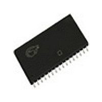
CY62128LL-70ZRC Cypress Semiconductor Corp, CY62128LL-70ZRC Datasheet

CY62128LL-70ZRC
Specifications of CY62128LL-70ZRC
Related parts for CY62128LL-70ZRC
CY62128LL-70ZRC Summary of contents
Page 1
... Cypress Semiconductor Corporation feature that reduces power consumption by more than 75% when deselected. Writing to the device is accomplished by taking chip enable one (CE ) and write enable (WE) inputs LOW and chip enable 1 two (CE ) input HIGH. Data on the eight I/O pins (I then written into the location specified on the address ...
Page 2
Selection Guide Maximum Access Time (ns) Maximum Operating Current Maximum CMOS Standby Current Maximum Ratings (Above which the useful life may be impaired. For user guide- lines, not tested.) Storage Temperature ................................. – +150 C Ambient Temperature with ...
Page 3
CY62128 ...
Page 4
Electrical Characteristics Over the Operating Range Parameter Description V Output HIGH Voltage OH V Output LOW Voltage OL V Input HIGH Voltage IH [1] V Input LOW Voltage IL I Input Load Current IX I Output Leakage Cur- OZ rent ...
Page 5
AC Test Loads and Waveforms R1 1800 5V OUTPUT OUTPUT R2 100 pF 990 INCLUDING JIG AND SCOPE (a) Equivalent to: THÉVENIN EQUIVALENT 639 1.77V OUTPUT [6] Switching Characteristics Over the Operating Range Parameter READ CYCLE t Read Cycle Time ...
Page 6
Data Retention Characteristics Parameter Description V VCC for Data Retention DR I Data Retention Current Coml. CCDR [3] t Chip Deselect to Data Retention Time CDR [3] t Operation Recovery Time R Switching Waveforms [11,12] Read Cycle No.1 ADDRESS DATA ...
Page 7
Switching Waveforms (continued) Write Cycle No Controlled ADDRESS DATA I/O Write Cycle No. 2 (WE Controlled, OE HIGH During Write) ADDRESS ...
Page 8
Switching Waveforms (continued) Write Cycle No.3 (WE Controlled, OE LOW) ADDRESS NOTE 16 DATAI/O t HZWE Truth Table I/O – I ...
Page 9
CY62128 ...
Page 10
... CY62128L 70SI CY62128L 70ZI CY62128L-70ZAI CY62128L-70ZRI CY62128LL 70SC CY62128LL 70ZC CY62128LL-70ZAC CY62128LL-70ZRC CY62128LL 70SI CY62128LL-70ZI CY62128LL-70ZAI CY62128LL-70ZRI Document #: 38–00524–B © Cypress Semiconductor Corporation, 1998. The information contained herein is subject to change without notice. Cypress Semiconductor Corporation assumes no responsibility for the use of any circuitry other than circuitry embodied in a Cypress Semiconductor product ...
Page 11
... Cypress Semiconductor Corporation, 1998. The information contained herein is subject to change without notice. Cypress Semiconductor Corporation assumes no responsibility for the use of any circuitry other than circuitry embodied in a Cypress Semiconductor product. Nor does it convey or imply any license under patent or other rights. Cypress Semiconductor does not authorize its products for use as critical components in life-support systems where a malfunction or failure may reasonably be expected to result in significant injury to the user ...
Page 12
... Package Diagrams © Cypress Semiconductor Corporation, 1998. The information contained herein is subject to change without notice. Cypress Semiconductor Corporation assumes no responsibility for the use of any circuitry other than circuitry embodied in a Cypress Semiconductor product. Nor does it convey or imply any license under patent or other rights. Cypress Semiconductor does not authorize its products for use as critical components in life-support systems where a malfunction or failure may reasonably be expected to result in significant injury to the user ...
Page 13
... Reverse Thin Small Outline Package ZR32 © Cypress Semiconductor Corporation, 1998. The information contained herein is subject to change without notice. Cypress Semiconductor Corporation assumes no responsibility for the use of any circuitry other than circuitry embodied in a Cypress Semiconductor product. Nor does it convey or imply any license under patent or other rights. Cypress Semiconductor does not authorize its products for use as critical components in life-support systems where a malfunction or failure may reasonably be expected to result in significant injury to the user ...


