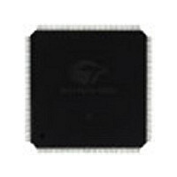
CY7C09579V-83AI Cypress Semiconductor Corp, CY7C09579V-83AI Datasheet - Page 2

CY7C09579V-83AI
Manufacturer Part Number
CY7C09579V-83AI
Description
Manufacturer
Cypress Semiconductor Corp
Datasheet
1.CY7C09579V-83AI.pdf
(32 pages)
Specifications of CY7C09579V-83AI
Density
1.125Mb
Access Time (max)
6ns
Sync/async
Synchronous
Architecture
SDR
Clock Freq (max)
45MHz
Operating Supply Voltage (typ)
3.3V
Address Bus
15b
Package Type
TQFP
Operating Temp Range
-40C to 85C
Number Of Ports
2
Supply Current
385mA
Operating Supply Voltage (min)
3.135V
Operating Supply Voltage (max)
3.465V
Operating Temperature Classification
Industrial
Mounting
Surface Mount
Pin Count
144
Word Size
36b
Number Of Words
32K
Lead Free Status / Rohs Status
Not Compliant
Functional Description
The CY7C09569V and CY7C09579V are high-speed 3.3 V
synchronous CMOS 16K and 32K × 36 dual-port static RAMs.
Two ports are provided, permitting independent, simultaneous
access for reads and writes to any location in memory. Registers
on control, address, and data lines allow for minimal set-up and
hold times. In pipelined output mode, data is registered for
decreased cycle time. Clock to data valid t
Flow-through mode can also be used to bypass the pipelined
output register to eliminate access latency. In flow-through mode
data will be available t
into the device. Pipelined output or flow-through mode is
selected via the FT/Pipe pin.
Each port contains a burst counter on the input address register.
The internal write pulse width is independent of the external R/W
LOW duration. The internal write pulse is self-timed to allow the
shortest possible cycle times.
Document Number: 38-06054 Rev. *D
CD1
= 12.5 ns after the address is clocked
CD2
= 5 ns (pipelined).
A HIGH on CE for one clock cycle will power down the internal
circuitry to reduce the static power consumption. In the pipelined
mode, one cycle is required with CE LOW to reactivate the
outputs.
Counter Enable Inputs are provided to stall the operation of the
address input and utilize the internal address generated by the
internal counter for fast interleaved memory applications. A
port’s burst counter is loaded with the port’s Address Strobe
(ADS). When the port’s Count Enable (CNTEN) is asserted, the
address counter will increment on each LOW-to-HIGH transition
of that port’s clock signal. This will read/write one word from/into
each successive address location until CNTEN is deasserted.
The counter can address the entire memory array and will loop
back to the start. Counter Reset (CNTRST) is used to reset the
burst counter.
All parts are available in 144-pin Thin Quad Plastic Flatpack
(TQFP), 144-pin Pb-free Thin Quad Plastic Flatpack (TQFP) and
172-ball Ball Grid Array (BGA) packages.
CY7C09569V
CY7C09579V
Page 2 of 32
[+] Feedback


