LM108AH National Semiconductor, LM108AH Datasheet - Page 3
LM108AH
Manufacturer Part Number
LM108AH
Description
Manufacturer
National Semiconductor
Type
General Purpose Amplifierr
Datasheet
1.LM108AH.pdf
(8 pages)
Specifications of LM108AH
Rail/rail I/o Type
No
Number Of Elements
1
Slew Rate
0.3V/us
Common Mode Rejection Ratio
96dB
Input Offset Voltage
500uV
Input Bias Current
2nA
Single Supply Voltage (typ)
Not RequiredV
Dual Supply Voltage (typ)
±3/±5/±9/±12/±15/±18V
Power Dissipation
500mW
Voltage Gain In Db
109.54dB
Power Supply Rejection Ratio
96dB
Power Supply Requirement
Dual
Shut Down Feature
No
Single Supply Voltage (min)
Not RequiredV
Single Supply Voltage (max)
Not RequiredV
Dual Supply Voltage (min)
±2V
Dual Supply Voltage (max)
±20V
Technology
Bipolar
Operating Temp Range
-55C to 125C
Operating Temperature Classification
Military
Mounting
Through Hole
Pin Count
8
Package Type
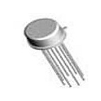
TO-99
Lead Free Status / Rohs Status
Not Compliant
Available stocks
Company
Part Number
Manufacturer
Quantity
Price

Part Number:
LM108AH
Manufacturer:
NS/国半
Quantity:
20 000
Company:
Part Number:
LM108AH/883
Manufacturer:
NSC
Quantity:
5 510
Part Number:
LM108AHRQV
Manufacturer:
NS/国半
Quantity:
20 000


LM308A Absolute Maximum Ratings
If Military Aerospace specified devices are required
please contact the National Semiconductor Sales
Office Distributors for availability and specifications
Supply Voltage
Power Dissipation (Note 1)
Differential Input Current (Note 2)
Input Voltage (Note 3)
Output Short-Circuit Duration
Operating Temperature Range
Storage Temperature Range
H-Package Lead Temperature
Electrical Characteristics
Note 1 The maximum junction temperature of the LM308A is 85 C For operating at elevated temperatures devices in the H08 package must be derated based on
a thermal resistance of 160 C W junction to ambient or 20 C W junction to case The thermal resistance of the dual-in-line package is 100 C W junction to
ambient
Note 2 The inputs are shunted with back-to-back diodes for overvoltage protection Therefore excessive current will flow if a differential input voltage in excess of
1V is applied between the inputs unless some limiting resistance is used
Note 3 For supply voltages less than
Note 4 These specifications apply for
of Input Offset Voltage
of Input Offset Current
Input Offset Voltage
Input Offset Current
Input Bias Current
Input Resistance
Supply Current
Large Signal Voltage Gain
Input Offset Voltage
Average Temperature Coefficient
Input Offset Current
Average Temperature Coefficient
Input Bias Current
Large Signal Voltage Gain
Output Voltage Swing
Input Voltage Range
Common Mode Rejection Ratio
Supply Voltage Rejection Ratio
(Soldering 10 sec )
Parameter
g
g
15V the absolute maximum input voltage is equal to the supply voltage
5V
s
V
S s g
b
T
T
T
T
T
T
V
V
V
V
R
V
V
(Note 4)
65 C to
A
A
A
A
A
A
OUT
S
S
S
S
S
15V and 0 C
L t
0 C to
e
e
e
e
e
e
e
e
e
e
e
Continuous
10 k
25 C
25 C
25 C
25 C
25 C V
25 C V
e
g
g
g
g
g
g
15V R
15V R
15V V
15V R
15V
500 mW
a
Conditions
g
a
10 mA
150 C
300 C
g
g
10V R
70 C
s
18V
15V
S
S
T
OUT
S
S
L
A s
e
e
e
e
e
L t
g
g
a
10 k
100
100
e
3
15V
15V
70 C unless otherwise specified
10 k
g
Lead Temperature (Soldering 10 sec ) (DIP)
Soldering Information
See An-450 ‘‘Surface Mounting Methods and Their Effect
on Product Reliability’’ for other methods of soldering sur-
face mount devices
ESD rating to be determined
10V
Dual-In-Line Package
Small Outline Package
Soldering (10 sec )
Vapor phase (60 sec )
Infrared (15 sec )
g
g
Min
10
80
60
96
96
13
14
g
Typ
300
110
110
0 3
0 2
1 5
0 3
2 0
2 0
40
14
Max
0 73
0 5
0 8
5 0
1 5
10
10
1
7
pA C
V mV
V mV
Units
M
260 C
260 C
215 C
220 C
mV
mA
mV
V C
nA
nA
nA
nA
dB
dB
V
V
Related parts for LM108AH
Image
Part Number
Description
Manufacturer
Datasheet
Request
R

Part Number:
Description:
Operational Amplifiers
Manufacturer:
National Semiconductor
Datasheet:
Part Number:
Description:
LM108/LM208/LM308 Operational Amplifiers; Package: TO-99; No of Pins: 8; Container: Tray
Manufacturer:
National Semiconductor
Part Number:
Description:
LM10 Operational Amplifier and Voltage Reference; Package: TO-5; No of Pins: 8; Qty per Container: 500; Container: Box
Manufacturer:
National Semiconductor
Part Number:
Description:
National Semiconductor [8-Bit D/A Converter]
Manufacturer:
National Semiconductor
Datasheet:
Part Number:
Description:
National Semiconductor [Media Coprocessor]
Manufacturer:
National Semiconductor
Datasheet:
Part Number:
Description:
Digitally Controlled Tone and Volume Circuit with Stereo Audio Power Amplifier, Microphone Preamp Stage and National 3D Sound
Manufacturer:
National Semiconductor
Datasheet:
Part Number:
Description:
Digitally Controlled Tone and Volume Circuit with Stereo Audio Power Amplifier, Microphone Preamp Stage and National 3D Sound
Manufacturer:
National Semiconductor
Datasheet:
Part Number:
Description:
AC97 Rev 2 Codec with Sample Rate Conversion and National 3D Sound
Manufacturer:
National Semiconductor
Part Number:
Description:
Manufacturer:
National Semiconductor
Datasheet:
Part Number:
Description:
Manufacturer:
National Semiconductor
Datasheet:
Part Number:
Description:
General Purpose, Low Voltage, Low Power, Rail-to-Rail Output Operational Amplifiers
Manufacturer:
National Semiconductor
Datasheet:
Part Number:
Description:
8-bit 20 MSPS flash A/D converter.
Manufacturer:
National Semiconductor
Datasheet:
Part Number:
Description:
Low Noise Quad Operational Amplifier
Manufacturer:
National Semiconductor
Datasheet: