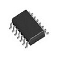
TC4066BFN Toshiba, TC4066BFN Datasheet - Page 2

TC4066BFN
Manufacturer Part Number
TC4066BFN
Description
Manufacturer
Toshiba
Type
Analog Switchr
Datasheet
1.TC4066BFN.pdf
(11 pages)
Specifications of TC4066BFN
Multiplexer Configuration
Quad SPST
Number Of Inputs
4
Number Of Outputs
4
Number Of Channels
4
Package Type
SOP
Power Supply Requirement
Single
Single Supply Voltage (min)
3V
Single Supply Voltage (typ)
5/9/12/15V
Single Supply Voltage (max)
18V
Dual Supply Voltage (min)
Not RequiredV
Dual Supply Voltage (typ)
Not RequiredV
Dual Supply Voltage (max)
Not RequiredV
Mounting
Surface Mount
Pin Count
14
Operating Temp Range
-40C to 85C
Operating Temperature Classification
Industrial
Lead Free Status / Rohs Status
Not Compliant
Available stocks
Company
Part Number
Manufacturer
Quantity
Price
Part Number:
TC4066BFN
Manufacturer:
TOSHIBA/东芝
Quantity:
20 000
Company:
Part Number:
TC4066BFN(ELF)
Manufacturer:
Toshiba
Quantity:
80 000
Logic Diagram
Absolute Maximum Ratings (Note)
Operating Ranges
DC supply voltage
Control input voltage
Switch I/O voltage
Potential difference across I/O during
ON
Control input current
Power dissipation
Operating temperature range
Storage temperature range
Note:
DC supply voltage
Input voltage
Note:
1/4 TC4066B
I/O
CONT
Exceeding any of the absolute maximum ratings, even briefly, lead to deterioration in IC performance or
even destruction.
Using continuously under heavy loads (e.g. the application of high temperature/current/voltage and the
significant change in temperature, etc.) may cause this product to decrease in the reliability significantly
even if the operating conditions (i.e. operating temperature/current/voltage, etc.) are within the absolute
maximum ratings and the operating ranges.
Please design the appropriate reliability upon reviewing the Toshiba Semiconductor Reliability Handbook
(“Handling Precautions”/“Derating Concept and Methods”) and individual reliability data (i.e. reliability test
report and estimated failure rate, etc).
The operating ranges must be maintained to ensure the normal operation of the device.
Unused control inputs must be tied to either V
Characteristics
Characteristics
(V
SS
= 0 V) (Note)
V
Symbol
Symbol
DD
V
V
V
T
V
I
T
I
P
CIN
I/O
/V
CIN
DD
opr
stg
DD
I/O
D
OUT
O/I
DD
2
V
V
or V
V
300 (DIP)/180 (SOIC)
SS
SS
SS
Test Condition
SS
− 0.5 to V
− 0.5 to V
− 0.5 to V
−65 to 150
−40 to 85
.
Rating
⎯
⎯
±0.5
±10
DD
DD
SS
+ 0.5
+ 0.5
+ 20
TC4066BP/BF/BFN/BFT
Min
3
0
Unit
mW
mA
°C
°C
V
V
V
V
Typ.
⎯
⎯
2007-10-01
V
Max
18
DD
Unit
V
V


