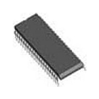
MM5483N National Semiconductor, MM5483N Datasheet - Page 3

MM5483N
Manufacturer Part Number
MM5483N
Description
Manufacturer
National Semiconductor
Datasheet
1.MM5483N.pdf
(8 pages)
Specifications of MM5483N
Operating Supply Voltage (typ)
3.3/5/9V
Number Of Digits
4.5
Number Of Segments
31
Operating Temperature (min)
-40C
Operating Temperature (max)
85C
Operating Temperature Classification
Industrial
Package Type
PDIP
Pin Count
40
Mounting
Through Hole
Power Dissipation
350mW
Frequency (max)
500KHz
Operating Supply Voltage (min)
3V
Operating Supply Voltage (max)
10V
Lead Free Status / Rohs Status
Not Compliant
Available stocks
Company
Part Number
Manufacturer
Quantity
Price
Company:
Part Number:
MM5483N
Manufacturer:
NSC
Quantity:
1 235
Part Number:
MM5483N
Manufacturer:
NS/国半
Quantity:
20 000
Power Supply
Average Supply Current, I
Input Voltage Levels
Output Current Levels
Segments and Data Out
BP Out Sink
BP Out Source
f
t
t
t
t
t
t
t
C
CH
CL
DS
DH
LW
LTC
CDO
Symbol
Absolute Maximum Ratings
If Military/Aerospace specified devices are required,
please contact the National Semiconductor Sales Office/
Distributors for availability and specifications.
DC Electrical Characteristics
T
Logic “0”
Logic “1”
Logic “0”
Logic “1”
Sink
Source
AC Electrical Characteristics
V
Note 1: “Absolute Maximum Ratings” are those values beyond which the safety of the device cannot be guaranteed. They are not meant to imply that the devices
should be operated at these limits. The table of “Electrical Characteristics” specifies conditions of device operation.
Note 2: AC input waveform specification for test purpose: t
Note 3: Clock input rise and fall times must not excced 300 ms.
Note 4: Output offset voltage is ±50 mV with C
Voltage at Any Pin
Operating Temperature
A
DD
within operating range, V
≥
4.7V, V
Parameter
Clock Frequency, V
Clock Period High
Clock Period Low
Data Set-Up before Clock
Data Hold Time after Clock
Minimum Load Pulse Width
Load to Clock
Clock to Data Valid
SS
= 0V unless otherwise specified
DD
DD
DD
= 3.0V to 10V, V
= 3V
All Outputs Bits = Open, Data Out = Open,
BP_Out = Open, Clock In = 0V,
Data In = 0V, Data Load = 0V,
Osc In = 0V, BP_In = 32Hz
V
V
V
Load, Clock, Data
V
V
V
V
V
V
V
V
DD
DD
DD
DD
DD
DD
DD
DD
DD
DD
DD
SEGMENT
= 3.0V
= 5.0V
= 10.0V
= 5.0V
= 5.0V
= 3.0V
= 3.0V
= 3.0V, V
= 3.0V, V
= 3.0V, V
= 3.0V, V
Parameter
V
−40°C to +85°C
SS
= 250 pF, C
r
to V
(Note 1)
SS
OUT
OUT
OUT
OUT
≤
= 0V, unless otherwise specified
20 ns, t
SS
Conditions
= 0.3V
= 2.7V
= 0.3V
= 2.7V
+10V
BP
f
= 8750 pF.
≤
20 ns, f = 500 kHz, 50% ± 10% duty cycle.
(Notes 2, 3)
3
Storage Temperature
Power Dissipation
Junction Temperature
Lead Temperature
(Soldering, 10 seconds)
Min
500
500
300
100
500
400
Min
320
320
3.0
2.4
2.0
20
20
Typ
400
Typ
1.5
Max
500
750
300 mW at +85°C
350 mW at +25°C
−65°C to +150°C
Max
2.5
0.9
0.4
10
10
40
www.national.com
+150°C
300°C
Units
Units
kHz
ns
ns
ns
ns
ns
ns
ns
µA
µA
µA
µA
µA
µA
µA
V
V
V
V
V


