PQ30RV11 Sharp Electronics, PQ30RV11 Datasheet - Page 7
PQ30RV11
Manufacturer Part Number
PQ30RV11
Description
Manufacturer
Sharp Electronics
Datasheet
1.PQ30RV11.pdf
(9 pages)
Specifications of PQ30RV11
Voltage Regulator Type
Linear
Topology
LDO
Regulator Output Type
Adjustable
Polarity Type
Positive
Number Of Outputs
Single
Input Voltage (min)
4.5V
Input Voltage (max)
35V
Output Voltage
1.5 to 30V
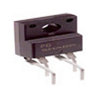
Package Type
TO-220
Output Current
1A
Power Dissipation
15W
Load Regulation
1%
Line Regulation
2.5%
Output Voltage Accuracy
±2%
Operating Temp Range
-20C to 80C
Operating Temperature Classification
Commercial
Dropout Voltage@current (max)
0.5@500mA
Pin Count
4 +Tab
Mounting
Through Hole
Quiescent Current (max)
7mA
Lead Free Status / Rohs Status
Not Compliant
Available stocks
Company
Part Number
Manufacturer
Quantity
Price
Company:

Part Number:
PQ30RV11
Manufacturer:
SHARP
Quantity:
214
Part Number:
PQ30RV11
Manufacturer:
SHARP
Quantity:
20 000


Low Power-Loss Voltage Regulators
V
ON/OFF operation is available by mounting externally D
When V
V
regulator is turned off). When the output is OFF, V
than maximum rating 7V.
In OFF-state, the load current flows to R
occurs at the load. OFF-state equivalent circuit R
range. In some case, as output voltage is getting lower(V
sometime impossible to obtain the minimum value of V
circuit parallel to the load.
IN
O
An Example of ON/OFF Circuit Using the 1-chip Microcomputer Output Port(PQ30RV1)
ON/OFF Operation
'=V
ADJ
<Specification>
Output port of microcomputer
Output should be set as follows.
From V
R
Assuming that V
V
If R
I
=1.6V (10k +114.8k )/10k
Hence, I
Next, assuming that V
I
Figure 1 shows the V
OH
OH
ADJ
2
ref
/R
=1.6V (R
=(5V–0.5V)(R
(max)=1.3V we get R
C
R
1
V
V
MAX. rating of I
15.6V R
=10k , we get R
is forcibly raised above V
IN
L
1
OH
OH
=11.48
/(R
1
O
(max)=0.5 V
(min)=2.4 V (I
OH
=1.25V(1+R
L
+R
<0.2mA. Therefore V
D
L
3
1
2
1
=52 (I
+R
)
V
2
F
ADJ
1
)/R
(max)=0.8V for D
+R
4
2
R
R
O
2
OH
2
2
O
1
)/R
2
1
/R
=11.48 R
=0.3A)
–V
OH
F
=0.5mA
R
(min)=0.5V for D
1
C
=0.2mA)
3
)we get V
2
1
=0
D
characteristics when R
R
2
R
3
2
ref
=0.49mA which is less than the rating.
1
(1.25V TYP)by applying the external signal, the output is turned off(pass transistor of
=114.8k and I
OH
114.8k =0.17mA
+
L
C
(min)is ensured.
O
2
O
from V
=15.6V.
V
in case of V
C
High : Output OFF
Low : Output ON
2
1
in case of V
R
ADJ
L
up to 10k is allowed. Select as high value of R
V
O
ADJ
through R
OH
OH
must be higher then V
1
O
=10k , R
(min)=2.4V, we get V
as follows, ingnoring R
'. So add the dummy resistance indicated by R
O
2
<1V), impedance of load resistance rises. In such condition, it is
and R
OH
2
(max), we get:
. Therefore the value of R
2
=115k , R
3
.
PQ30RV1/PQ30RV11/PQ30RV2/PQ30RV21
3
=0 , V
R
1
ADJ
ref
Equivalent Circuit
in OFF-state
L
MAX., and at the same time must be lower
=V
V
(52 ):
ADJ
IN
OH
=17V, R
R
R
2
(min)–V
L
D
2
V
must be as high as possible.
2
O
L
'
=52 , and D
F
(max)=2.4V–0.8V=1.6V. From
R
L
D
and R
D
2
1
in the figure to the
=1S2076A(Hitachi).
as possible in this
Related parts for PQ30RV11
Image
Part Number
Description
Manufacturer
Datasheet
Request
R

Part Number:
Description:
Manufacturer:
Sharp Electronics
Datasheet:
Part Number:
Description:
Manufacturer:
Sharp Electronics
Datasheet:
Part Number:
Description:
Manufacturer:
Sharp Electronics
Datasheet:
Part Number:
Description:
Manufacturer:
Sharp Electronics
Datasheet:

Part Number:
Description:
Manufacturer:
Sharp Electronics
Datasheet:
Part Number:
Description:
Manufacturer:
Sharp Electronics
Datasheet:
Part Number:
Description:
Manufacturer:
Sharp Electronics
Datasheet:


Part Number:
Description:
Manufacturer:
Sharp Electronics
Datasheet:
Part Number:
Description:
Manufacturer:
Sharp Electronics
Datasheet: