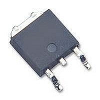
AUIRFR2407 International Rectifier, AUIRFR2407 Datasheet - Page 2

AUIRFR2407
Manufacturer Part Number
AUIRFR2407
Description
54T8894
Manufacturer
International Rectifier
Datasheet
1.AUIRFR2407.pdf
(12 pages)
Specifications of AUIRFR2407
Transistor Polarity
N Channel
Continuous Drain Current Id
42A
Drain Source Voltage Vds
75V
On Resistance Rds(on)
0.0218ohm
Rds(on) Test Voltage Vgs
10V
Power Dissipation Pd
110W
Rohs Compliant
Yes
Drain-source Breakdown Voltage
75 V
Gate-source Breakdown Voltage
20 V
Continuous Drain Current
42 A
Power Dissipation
110 W
Mounting Style
SMD/SMT
Package / Case
DPAK
Gate Charge Qg
74 nC
Lead Free Status / Rohs Status
Details
Available stocks
Company
Part Number
Manufacturer
Quantity
Price
Company:
Part Number:
AUIRFR2407
Manufacturer:
IR
Quantity:
12 500
Repetitive rating; pulse width limited by
‚ Starting T
ƒ I
„ Pulse width ≤ 300μs; duty cycle ≤ 2%.
Static Electrical Characteristics @ T
V
ΔV
R
V
gfs
I
I
Dynamic Electrical Characteristics @ T
Q
Q
Q
t
t
t
t
L
L
C
C
C
C
C
C
I
I
V
t
Q
t
Diode Characteristics
DSS
GSS
d(on)
r
d(off)
f
S
SM
rr
on
D
S
(BR)DSS
GS(th)
SD
DS(on)
g
gs
gd
iss
oss
rss
oss
oss
oss
rr
2
(BR)DSS
R
T
max. junction temperature.
SD
J
G
eff.
≤ 175°C.
= 25Ω, I
≤ 25A, di/dt ≤ 290A/μs, V
/ΔT
J
J
= 25°C, L = 0.42mH
AS
Drain-to-Source Breakdown Voltage
Breakdown Voltage Temp. Coefficient
Static Drain-to-Source On-Resistance
Gate Threshold Voltage
Forward Transconductance
Drain-to-Source Leakage Current
Gate-to-Source Forward Leakage
Gate-to-Source Reverse Leakage
Total Gate Charge
Gate-to-Source Charge
Gate-to-Drain ("Miller") Charge
Turn-On Delay Time
Rise Time
Turn-Off Delay Time
Fall Time
Internal Drain Inductance
Internal Source Inductance
Input Capacitance
Output Capacitance
Reverse Transfer Capacitance
Output Capacitance
Output Capacitance
Effective Output Capacitance
Continuous Source Current
(Body Diode)
Pulsed Source Current
(Body Diode)
Diode Forward Voltage
Reverse Recovery Time
Reverse Recovery Charge
Forward Turn-On Time
= 25A.
Parameter
Ù
Parameter
Parameter
DD
≤ V
(BR)DSS
,
J
= 25°C (unless otherwise specified)
… C
† When mounted on 1" square PCB (FR-4 or G-10 Material) .
‡ R
J
= 25°C (unless otherwise specified)
as C
For recommended footprint and soldering techniques refer to
application note #AN-994.
Intrinsic turn-on time is negligible (turn-on is dominated by LS+LD)
Min. Typ. Max. Units
Min. Typ. Max. Units
Min. Typ. Max. Units
oss
θ
–––
–––
–––
–––
–––
–––
–––
–––
–––
–––
–––
–––
–––
–––
–––
–––
–––
–––
–––
–––
–––
–––
–––
–––
–––
–––
2.0
75
27
is measured at T
oss
eff. is a fixed capacitance that gives the same charging time
while V
15700
0.078
2400
21.8
–––
–––
–––
–––
–––
–––
–––
340
220
220
–––
–––
–––
100
400
4.5
7.5
74
13
22
16
90
65
66
77
DS
-200
26.0
–––
–––
–––
250
200
110
–––
–––
–––
–––
–––
–––
–––
–––
–––
–––
–––
–––
170
150
600
4.0
1.3
20
19
34
42
is rising from 0 to 80% V
J
of approximately 90°C.
V/°C
mΩ
μA
nA
nC
nH
nC
pF
ns
ns
V
V
S
A
V
V
Reference to 25°C, I
V
V
V
V
V
V
V
I
V
V
V
I
R
V
Between lead,
6mm (0.25in.)
from package
and center of die contact
V
V
ƒ = 1.0MHz, See Fig. 5
V
V
V
MOSFET symbol
showing the
integral reverse
p-n junction diode.
T
T
di/dt = 100A/μs
D
D
J
J
GS
GS
DS
DS
DS
DS
GS
GS
DS
GS
DD
G
GS
GS
DS
GS
GS
GS
= 25A
= 25A
= 25°C, I
= 25°C, I
= 6.8Ω
= V
= 25V, I
= 75V, V
= 60V, V
= 60V
= 38V
= 25V
= 0V, I
= 10V, I
= 20V
= -20V
= 10V
= 10V
= 0V
= 0V, V
= 0V, V
= 0V, V
GS
, I
D
f
f
Conditions
Conditions
Conditions
DSS
D
DS
S
F
D
D
DS
DS
= 250μA
GS
GS
= 250μA
= 25A
= 25A, V
= 25A
= 25A
= 0V to 60V
= 1.0V, ƒ = 1.0MHz
= 60V, ƒ = 1.0MHz
.
= 0V
= 0V, T
f
www.irf.com
f
D
f
= 1mA
G
GS
J
= 150°C
= 0V
G
f
D
S
S
D


