J212-E3 Vishay, J212-E3 Datasheet - Page 3
J212-E3
Manufacturer Part Number
J212-E3
Description
51K2093
Manufacturer
Vishay
Datasheet
1.J211-E3.pdf
(7 pages)
Specifications of J212-E3
Power Dissipation Pd
350mW
Transistor Polarity
N Channel
Current Rating
10mA
Continuous Drain Current Id
40mA
Gate-source Breakdown Voltage
-25V
Leaded Process Compatible
Yes
Rohs Compliant
Yes
Gate-source Cutoff Voltage
-6V


Document Number: 70234
S-04028—Rev. E, 04-Jun-01
200
160
120
50
40
30
20
10
80
40
5
4
3
2
1
0
0
0
0
0
0
On-Resistance and Output Conductance
I
g
f = 1 kHz
DSS
I
fs
DSS
Drain Current and Transconductance
V
g
@ V
V
GS(off)
fs
@ V
vs. Gate-Source Cutoff Voltage
GS(off)
V
0.2
vs. Gate-Source Cutoff Voltage
–2
–2
GS(off
DS
V
DS
Output Characteristics
= –2 V
DS
= 10 V, V
)
– Gate-Source Cutoff Voltage (V)
r
g
f = 1 kHz
= 10 V, V
DS
– Gate-Source Cutoff Voltage (V)
os
– Drain-Source Voltage (V)
@ I
@ V
0.4
–4
–4
D
GS
DS
= 1 mA, V
GS
= 0 V
= 10 V, V
= 0 V
0.6
–6
–6
V
GS
GS
GS
g
r
DS
= 0 V
os
= 0 V
= 0 V
0.8
–8
–8
–0.2 V
–0.4 V
–0.6 V
–0.8 V
–1.0 V
–1.2 V
–10
_
–10
1
20
16
12
8
4
0
200
160
120
80
40
0
100 nA
100 pA
0.1 pA
10 pA
10 nA
1 nA
1 pA
10
8
6
4
2
0
15
12
9
6
3
0
0
Common-Source Forward Transconductance
0.1
0
I
V
T
G(on)
I
T
GSS
A
A
GS(off)
= 125_C
= 25_C
@ I
@ 125_C
V
GS(off)
4
= –5 V
0.2
V
D
DG
Gate Leakage Current
–2.0 V
V
Output Characteristics
= –5 V
– Drain-Gate Voltage (V)
DS
I
vs. Drain Current
D
J/SSTJ210 Series
– Drain-Source Voltage (V)
25_C
– Drain Current (mA)
8
0.4
10 mA
–1.5 V
1 mA
Vishay Siliconix
–1.0 V
1
10 mA
T
12
–0.5 V
A
0.6
= –55_C
I
GSS
V
f = 1 kHz
125_C
DS
V
@ 25_C
GS
= 10 V
16
www.vishay.com
1 mA
0.8
= 0 V
–3.5 V
–2.5 V
–3.0 V
20
10
7-3
1
Related parts for J212-E3
Image
Part Number
Description
Manufacturer
Datasheet
Request
R

Part Number:
Description:
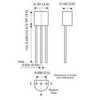
TRANSISTOR,JFET,N-Channel,40mA I(DSS),TO-92
Manufacturer:
Vishay
Part Number:
Description:
357-036-542-201 CARDEDGE 36POS DL .156 BLK LOPRO
Manufacturer:
Vishay
Datasheet:
Part Number:
Description:
357-036-542-201 CARDEDGE 36POS DL .156 BLK LOPRO
Manufacturer:
Vishay
Datasheet:
Part Number:
Description:
357-036-542-201 CARDEDGE 36POS DL .156 BLK LOPRO
Manufacturer:
Vishay
Datasheet:
Part Number:
Description:
357-036-542-201 CARDEDGE 36POS DL .156 BLK LOPRO
Manufacturer:
Vishay
Datasheet:
Part Number:
Description:
357-036-542-201 CARDEDGE 36POS DL .156 BLK LOPRO
Manufacturer:
Vishay
Datasheet:
Part Number:
Description:
357-036-542-201 CARDEDGE 36POS DL .156 BLK LOPRO
Manufacturer:
Vishay
Datasheet:
Part Number:
Description:
357-036-542-201 CARDEDGE 36POS DL .156 BLK LOPRO
Manufacturer:
Vishay
Datasheet:
Part Number:
Description:
357-036-542-201 CARDEDGE 36POS DL .156 BLK LOPRO
Manufacturer:
Vishay
Datasheet:
Part Number:
Description:
357-036-542-201 CARDEDGE 36POS DL .156 BLK LOPRO
Manufacturer:
Vishay
Datasheet:
Part Number:
Description:
357-036-542-201 CARDEDGE 36POS DL .156 BLK LOPRO
Manufacturer:
Vishay
Datasheet:
Part Number:
Description:
357-036-542-201 CARDEDGE 36POS DL .156 BLK LOPRO
Manufacturer:
Vishay
Datasheet:
Part Number:
Description:
357-036-542-201 CARDEDGE 36POS DL .156 BLK LOPRO
Manufacturer:
Vishay
Datasheet:
Part Number:
Description:
357-036-542-201 CARDEDGE 36POS DL .156 BLK LOPRO
Manufacturer:
Vishay
Datasheet:
Part Number:
Description:
357-036-542-201 CARDEDGE 36POS DL .156 BLK LOPRO
Manufacturer:
Vishay
Datasheet: